Wafer processing system, coating/developing apparatus, and wafer, processing apparatus

a technology of processing system and wafer, which is applied in the direction of charge manipulation, instruments, furniture, etc., can solve the problems of inability to meet the throughput of the aligner, adversely affecting the result of the development process, and deteriorating the yield of the final produ

Inactive Publication Date: 2005-12-29
TOKYO ELECTRON LTD
View PDF4 Cites 44 Cited by
  • Summary
  • Abstract
  • Description
  • Claims
  • Application Information

AI Technical Summary

Benefits of technology

[0014] In view of the foregoing, it would be desirable to provide an apparatus of which a processing unit processes a substrate, a transferring means transfers the wafer to another processing unit, and another transferring means transfers the wafer to a plurality of downstream processing units, in particular, to keep times after one processing unit processes substrate until another pro...

Problems solved by technology

After the wafer W is processed in the ADH, in reality, a temperature controlling process is preformed for the wafer W. However, due to the limited space of the drawing, the temperature controlling process is omitted.
When a chemically amplifying resist is used for fine patterns, it is thought that after the resist is exposed, the...

Method used


Image

  • Wafer processing system, coating/developing apparatus, and wafer, processing apparatus
  • Wafer processing system, coating/developing apparatus, and wafer, processing apparatus
  • Wafer processing system, coating/developing apparatus, and wafer, processing apparatus

Examples


Embodiment Construction

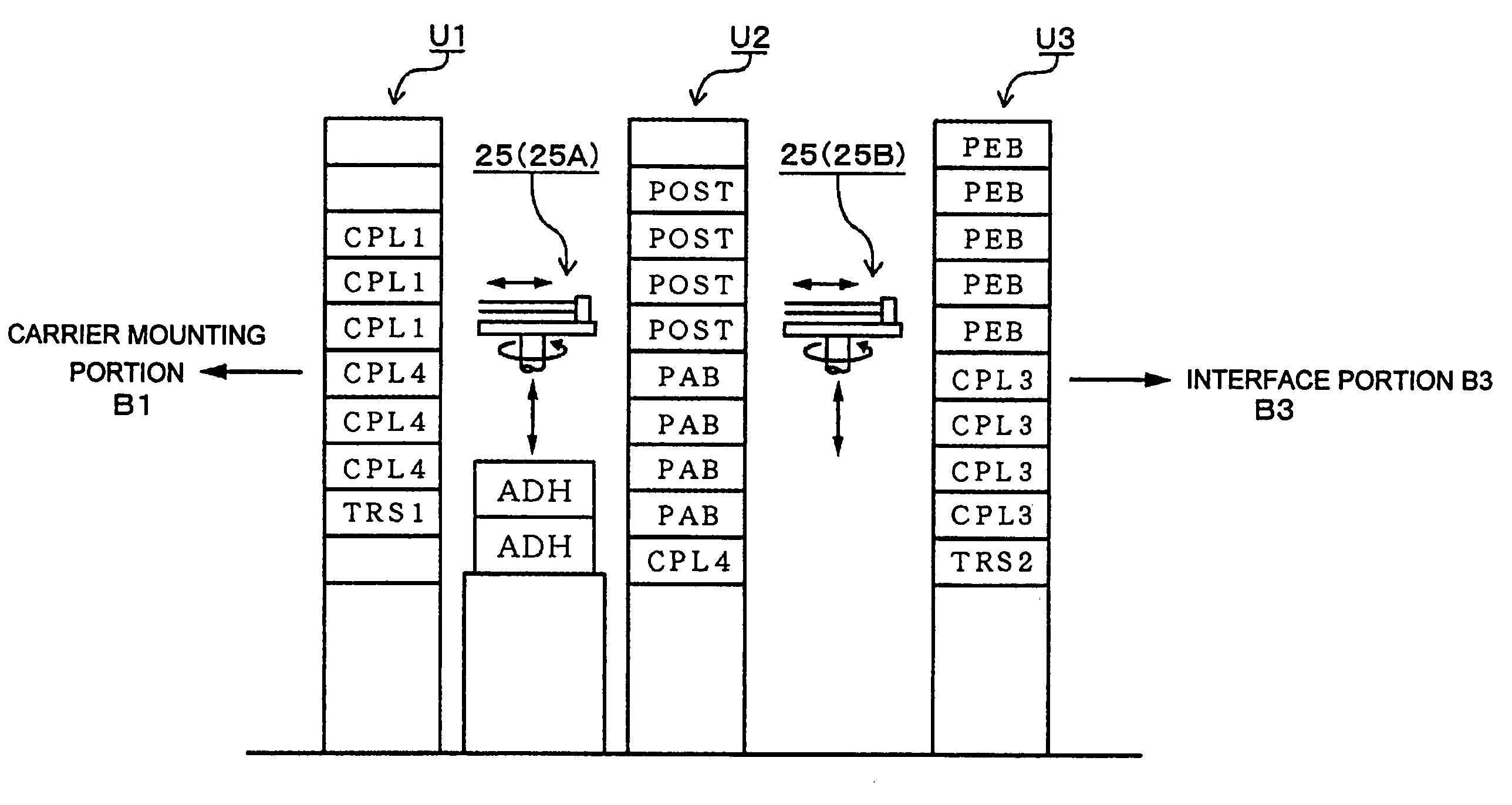
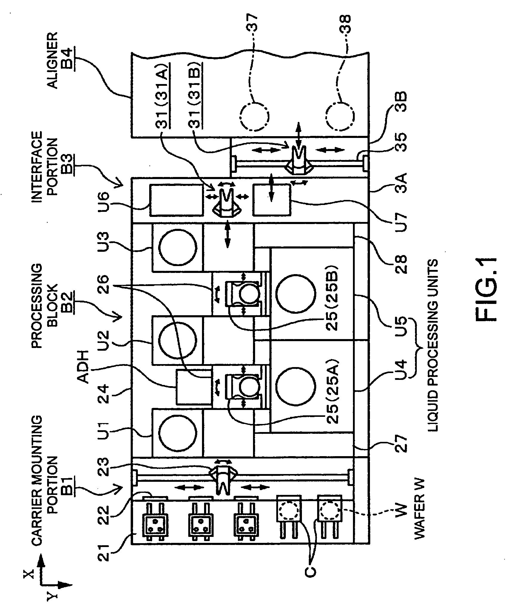
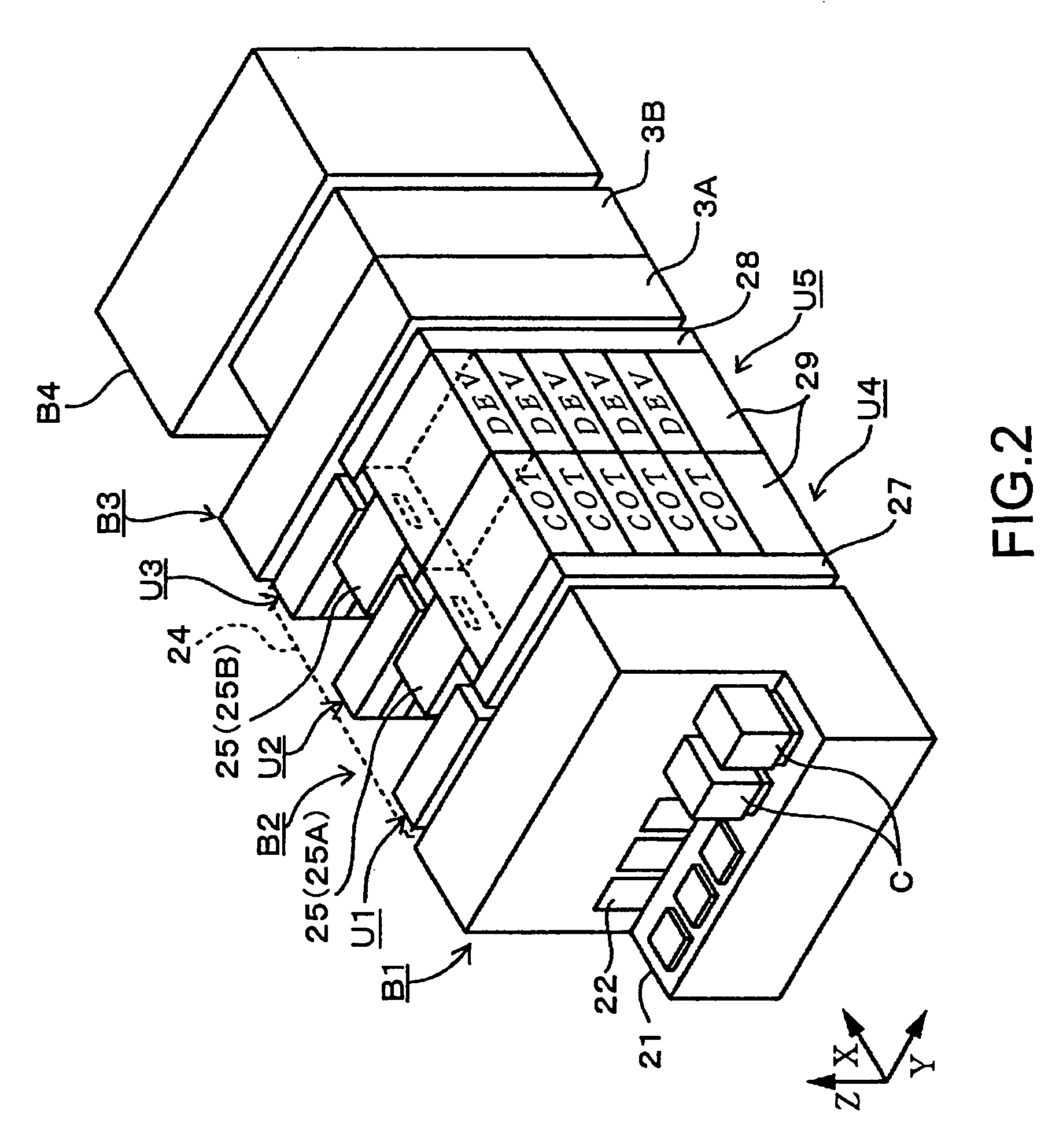
[0052] Next, a resist pattern forming apparatus to which a substrate processing system according to an embodiment of the present invention is applied will be described. The resist pattern forming apparatus as the coating and developing apparatus according to the embodiment of the present invention is composed of the coating and developing apparatus and an aligner. FIG. 1 is a plan view showing a resist pattern forming apparatus according to the embodiment. FIG. 2 is a perspective view showing the resist pattern forming apparatus. In these drawings, B1 represents a carrier mounting portion to and from which carriers C each of which airtightly contains for example 13 wafers W as workpieces are loaded and unloaded. The carrier mounting portion B1 has a table 21 on which a plurality of carriers can be placed, an open / close portion 22 formed disposed in a wall surface in the front of the table 21, and a transfer arm 23 that functions as a part of a first transferring means 1 that takes o...


PUM


Abstract

In a coating and developing apparatus that forms a resist film on substrates such as semiconductor wafers, and develops substrates exposed by an aligner, times after the aligner unloads substrates until heating units (PEB) start heating the substrates are kept uniform. Exposed wafers are prevented from being left stagnant in an interface portion disposed between a region in which resist is coated and developed and the aligner. In the region in which resist is coated and developed, a first transferring means that successively executes transportation cycles to transfer substrates from upstream side modules to downstream side modules in a flow of processes of substrates. N heating units (PEB) are disposed (n is for example 5). Exposed wafers loaded into the heating units (PEB) are unloaded by the first transferring means after (n−1) cycles including the transferring cycle of the first transferring means have elapsed.

Description

BACKGROUND OF THE INVENTION [0001] 1. Field of the Invention [0002] The present invention relates to a coating and developing apparatus of which a processing unit processes a substrate such as a semiconductor wafer or a liquid crystal display glass substrate (an LCD substrates), one transferring means transfers the substrate to another transferring means through a processing unit, and the other transferring means transfers the substrate to a plurality of downstream processing units. For example, the present invention relates to a coating and developing apparatus that forms a resist film on a substrate and performs a developing process for the exposed substrate, in particular to a transferring technology of an interface portion that is disposed between the apparatus and an aligner and that transfers an exposed substrate to a region in which a developing process is performed. [0003] 2. Description of the Related Art [0004] In a manufacturing process for semiconductor devices and LCD s...

Claims


Application Information

Patent Timeline
IPC IPC(8): G03F7/16G03F7/30H01L21/00
CPCG03F7/168H01L21/67276H01L21/67178G03F7/3021H01L21/67011H01L21/67703H01L21/67781
Inventor HIGASHI, MAKIOMIYATA, AKIRA
Owner TOKYO ELECTRON LTD
Why Eureka
Try Eureka