

Ramp waveform generation circuit, analog/digital conversion circuit, imaging device and control method of imaging device
a waveform generation and analog/digital conversion technology, applied in code conversion, instruments, television systems, etc., can solve the problems of inability to recognize the waveform generation circuit configured to be connected to both the cds circuit and the ads circuit at all, and the fixed pattern noise of the cmos image sensor, so as to improve the image quality of the optical/electrical conversion signal. , the effect of high accuracy
- Summary
- Abstract
- Description
- Claims
- Application Information
AI Technical Summary
Benefits of technology
Problems solved by technology
Method used
Image

Examples
Embodiment Construction
[0032] The preferred embodiments of the present invention are described in detail below with reference to the drawings.
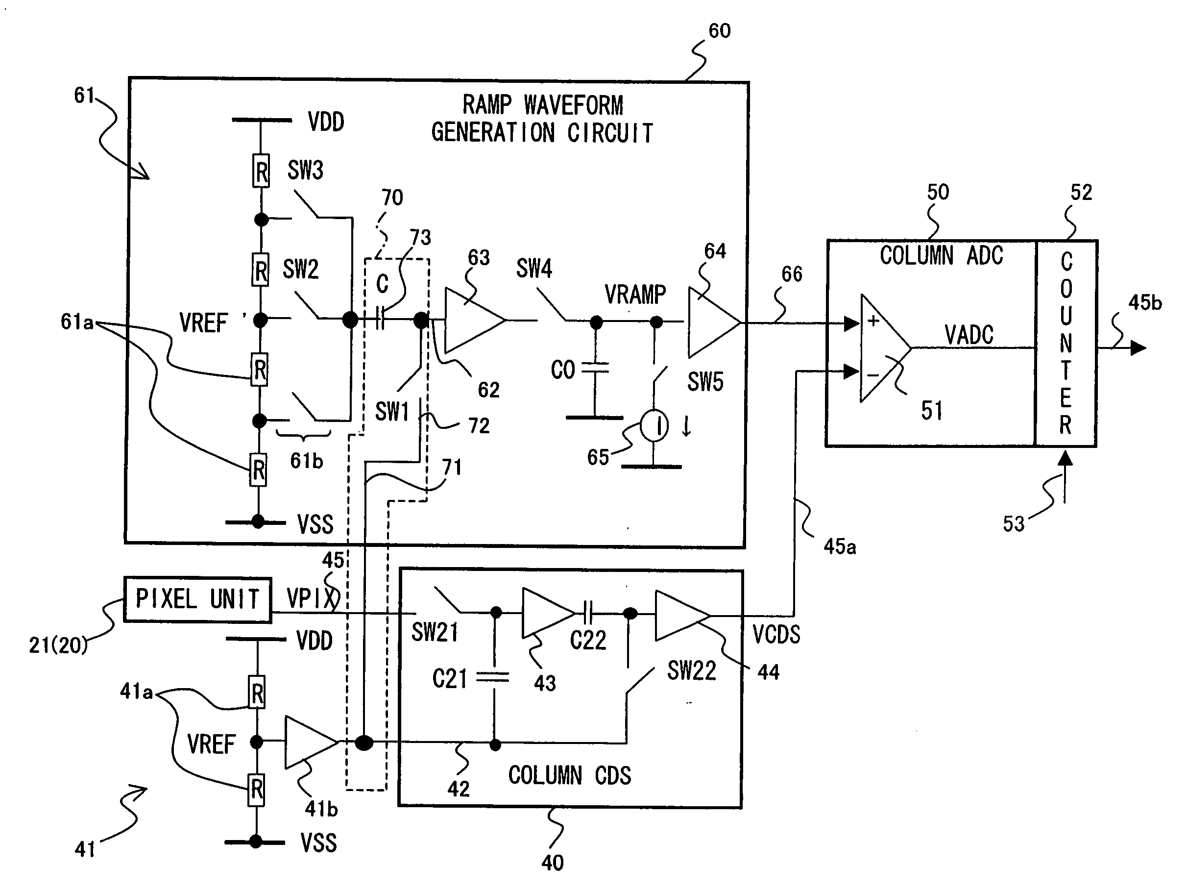
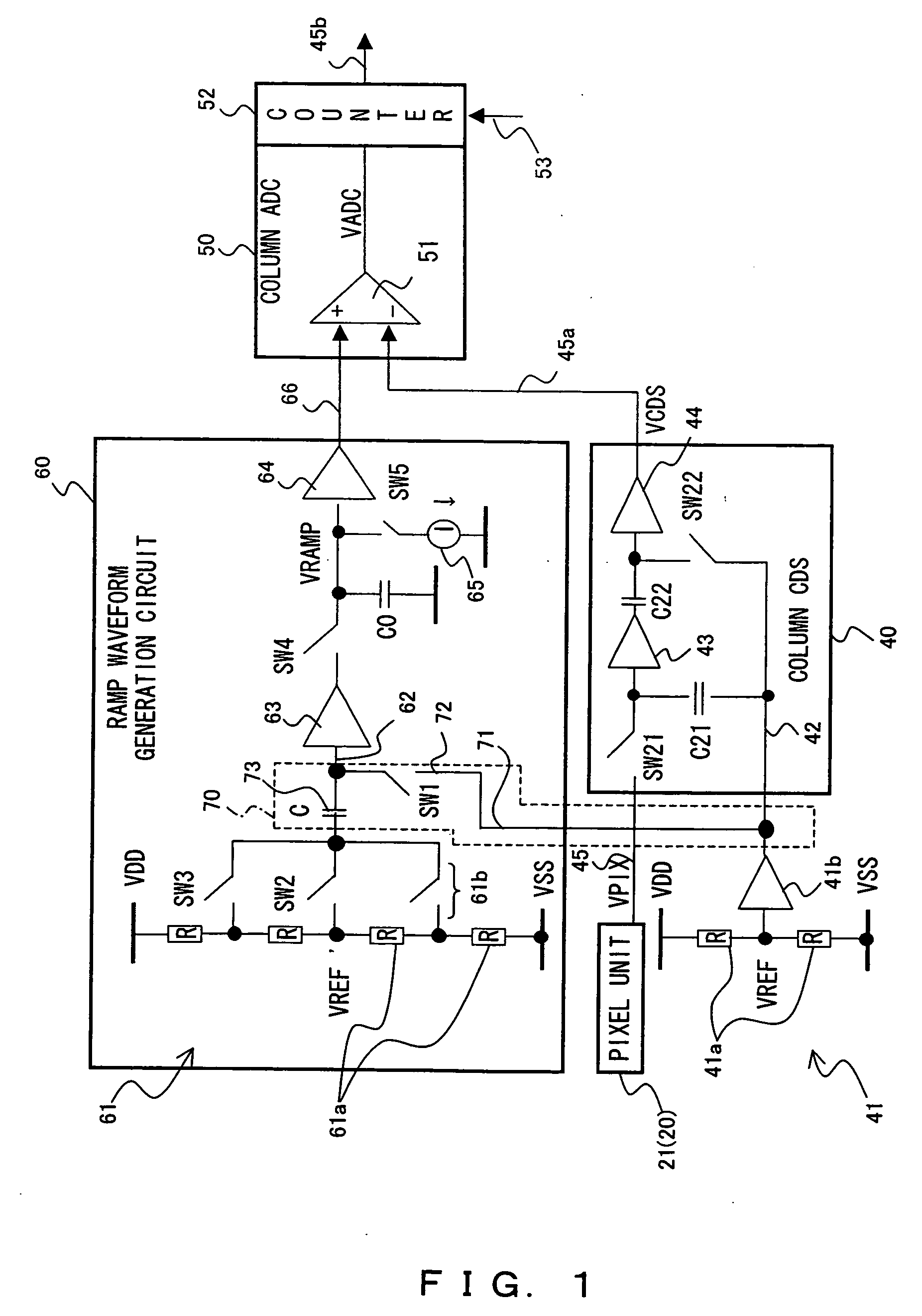
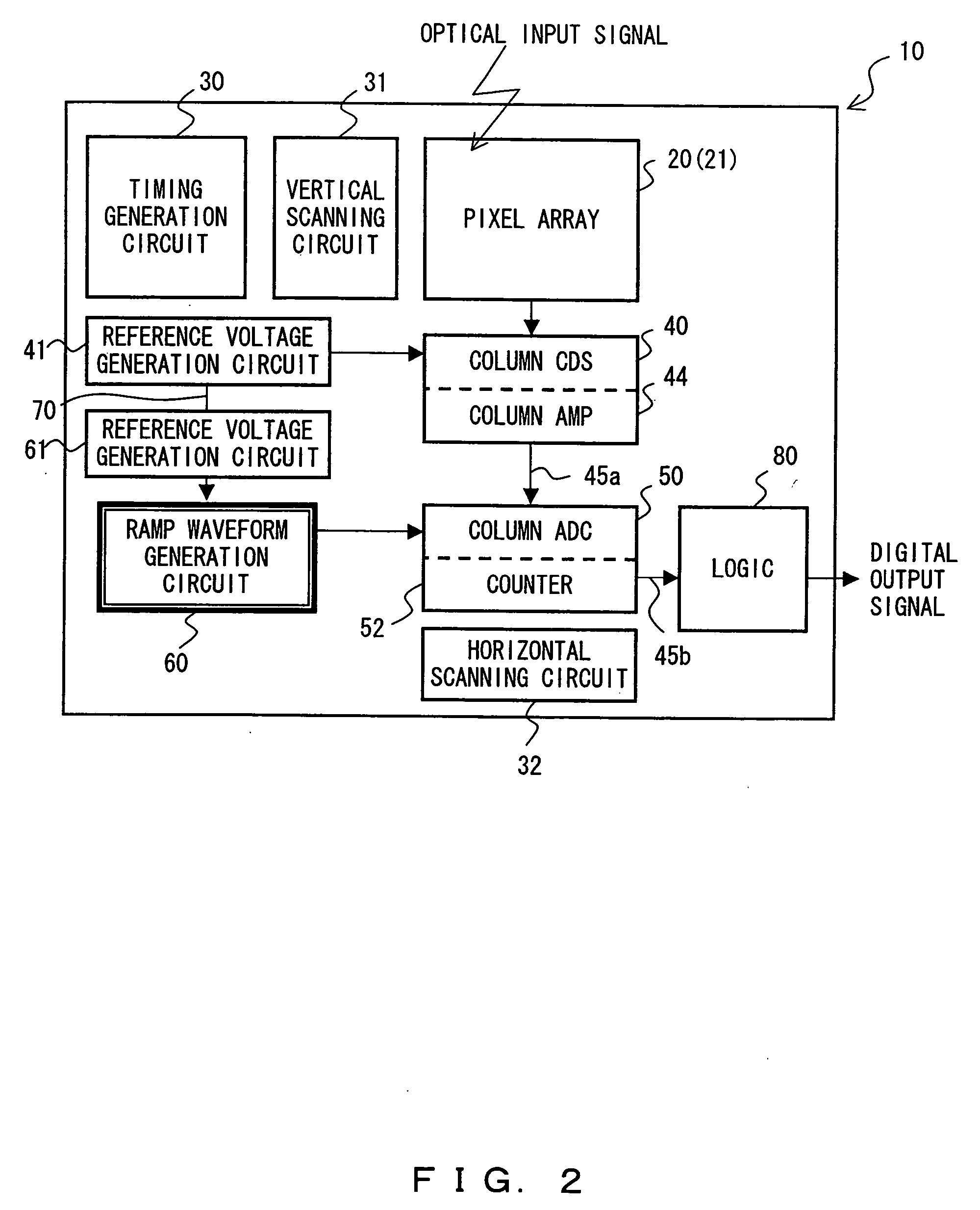
[0033]FIG. 1 is a circuit diagram showing an internal configuration of the imaging device which is one preferred embodiment of the present invention. FIG. 2 is a block diagram showing an entire configuration of the imaging device provided with a ramp waveform generation circuit and an analog / digital conversion device each of which is one preferred embodiment of the present invention. FIG. 3 is a timing chart showing an example of the function of each unit of the imaging device which is one preferred embodiment of the present invention. This preferred embodiment is described using a case where the present invention is applied to a CMOS image sensor as one example of the imaging device.
[0034] As shown in FIG. 2, an imaging device 10 in this preferred embodiment comprises a pixel array 20 in which a plurality of pixel units 21 each composed of an optical / electrical c...
PUM
 Abstract
Description
Claims
Application Information