Flat panel light emitting devices with two sided

a technology of light-emitting devices and flat panels, which is applied in the direction of discharge tubes/lamp details, discharge tubes luminescnet screens, electric discharge lamps, etc., can solve the problems of limiting utility, unable to provide for differentiated colors or images to be generated on opposite sides of flat-panel displays

Inactive Publication Date: 2006-01-12
EASTMAN KODAK CO
View PDF14 Cites 75 Cited by
  • Summary
  • Abstract
  • Description
  • Claims
  • Application Information

AI Technical Summary

Benefits of technology

[0004] In accordance with one embodiment, the present invention is directed towards a flat panel light emitting device comprised of a transparent substrate, a first organic light emitting diode element disposed over the substrate, a second organic light emitting diode element disposed over the first organic light emitting diode element, and a transparent cover disposed over the second organic light emitting element, wherein each of the first and second light emitting elements comprises an organic light emitting layer...

Problems solved by technology

Although enabling two-sided emission, the use of a single emission layer results in substantially the same image being provided on both sides, and the lack of independent control...

Method used


Image

  • Flat panel light emitting devices with two sided
  • Flat panel light emitting devices with two sided
  • Flat panel light emitting devices with two sided

Examples


Embodiment Construction

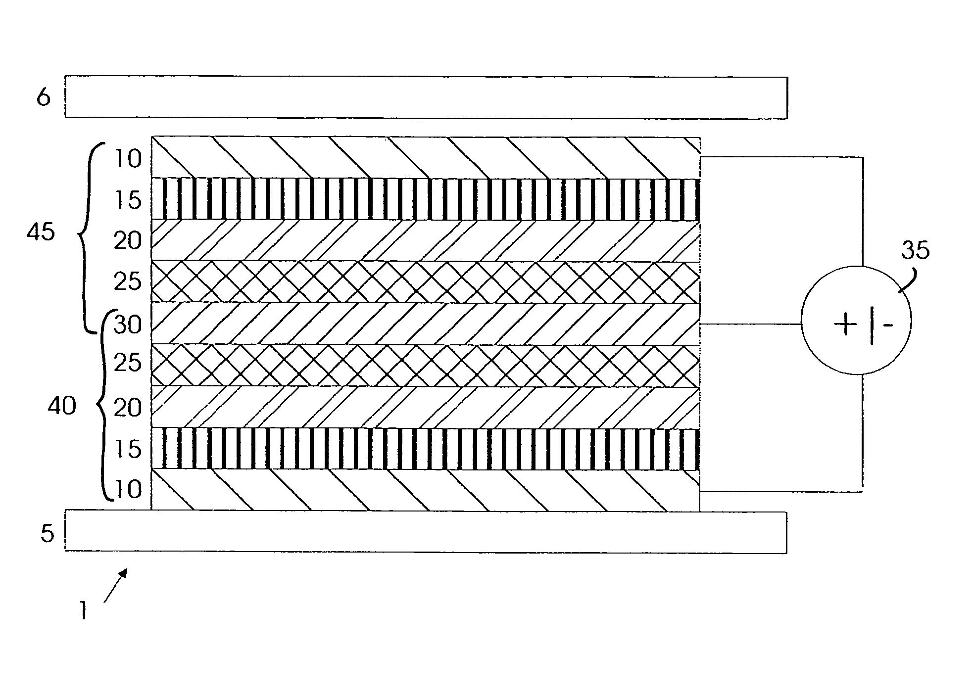
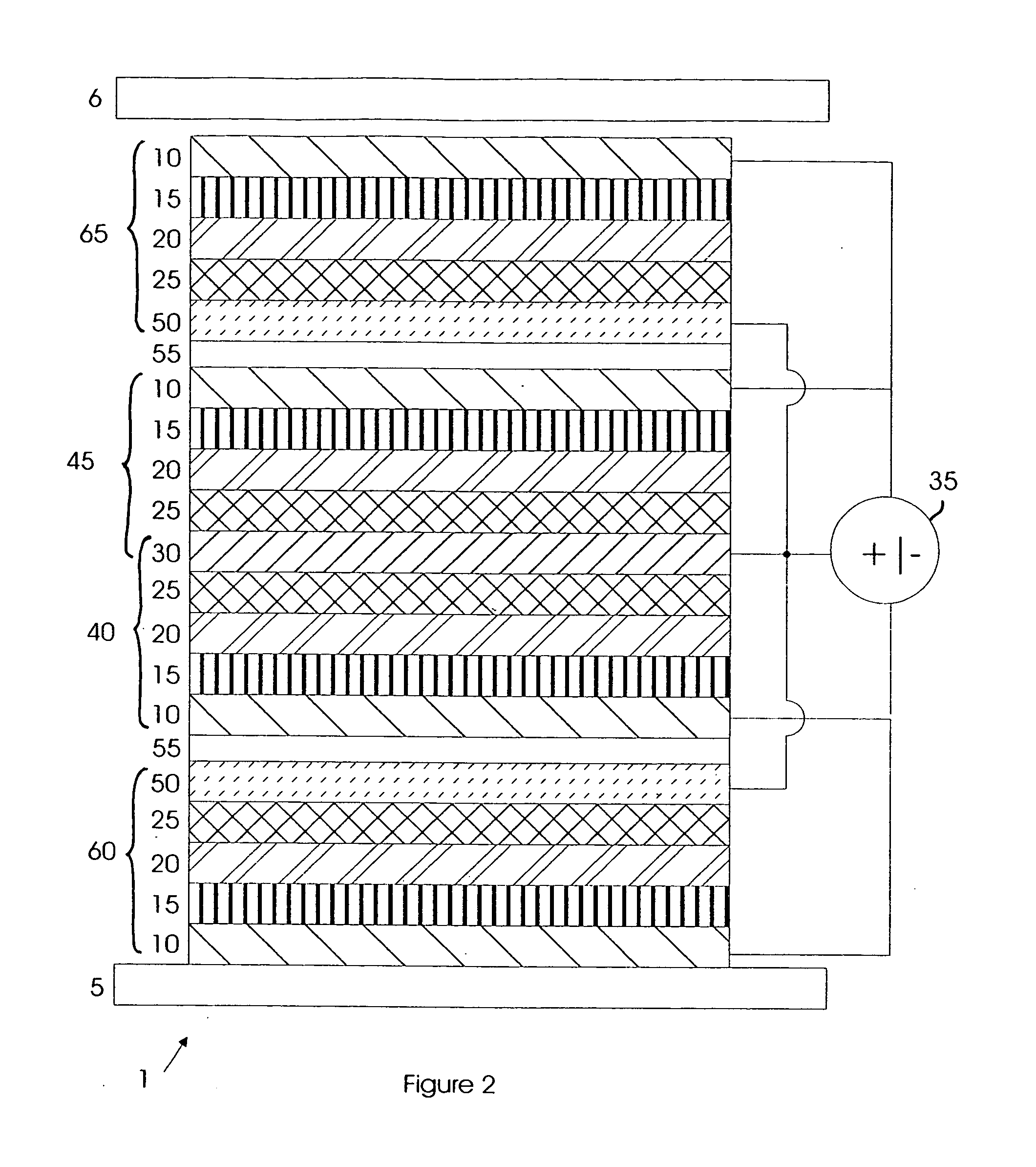
[0011] Referring to FIG. 1, a flat panel light emitting device 1 is constructed by depositing two organic light emitting diode (OLED) elements 40 and 45 on a transparent substrate 5 and covering the assembly with a transparent cover 6. In this specific embodiment, light emitting element 40 is constructed by the sequential deposition of thin film layers consisting of a transparent or semitransparent electrode 10 as an anode, a hole injection layer 15, an organic light emitting layer 20, an electron injection layer 25, and a reflective electrode layer 30 as a cathode. The order of layers is then reversed to create light emitting element 45. Electrodes 10 and 30 are connected to power supply 35. It is well-known that the light emitter layer 20 may contain multiple dopants or contain sublayers to control the emission spectrum.

[0012] The flat panel light emitting device 1 differs in two significant ways from the devices taught in U.S. Pat. No. 5,703,436 and JP06176870A. In particular, t...


PUM


Abstract

A flat panel light emitting device is descried comprised of a transparent substrate, a first organic light emitting diode element disposed over the substrate, a second organic light emitting diode element disposed over the first organic light emitting diode element, and a transparent cover disposed over the second organic light emitting element, wherein each of the first and second light emitting elements comprises an organic light emitting layer positioned between a transparent or semitransparent electrode and a reflective electrode, and wherein the first light emitting element emits light through its transparent or semitransparent electrode and the substrate and the second light emitting element emits light through its transparent or semitransparent electrode and the cover. The flat panel light emitting device is advantageous because it provides the capability to emit independently controlled patterns, colors, and intensities from the two sides of the flat panel.

Description

FIELD OF THE INVENTION [0001] The present invention relates to the manufacture of flat panel light emitting devices such as displays and extended light sources, an example being organic light emitting diode displays and area illumination sources and, more particularly, to the said devices capable of emitting distinct light patterns and colors on the two faces of the flat panel. BACKGROUND OF THE INVENTION [0002] Light emitting flat panel devices are used for a number of applications such as general illumination light sources, decorative light sources, and information displays. U.S. Pat. No. 5,703,436 discloses various embodiments, including an organic light emitting diode (OLED) display (FIG. 17 thereof) that emits light through both sides of the display through use of an electroluminescent material layer between transparent anode and cathode layers. Although enabling two-sided emission, the use of a single emission layer results in substantially the same image being provided on bot...

Claims


Application Information

Patent Timeline
IPC IPC(8): H01J1/62
CPCH01L27/3209H01L27/3286H01L27/3267H10K59/32H10K59/128H10K59/176
Inventor STRIP, DAVID R.
Owner EASTMAN KODAK CO
Why Eureka
Try Eureka