Liquid crystal display apparatus having level conversion circuit

a technology of level conversion circuit and liquid crystal display, which is applied in the direction of box making operation, instrumentation, pulse technique, etc., can solve the problem that the equivalent load capacity increase becomes an obstacle to achieve high speed operation, and achieve the effect of reducing the size of the transistor and high speed

Inactive Publication Date: 2006-01-12
PANASONIC LIQUID CRYSTAL DISPLAY CO LTD +1
View PDF1 Cites 19 Cited by
  • Summary
  • Abstract
  • Description
  • Claims
  • Application Information

AI Technical Summary

Benefits of technology

[0019] To obtain the resistance under the conductive state necessary for a voltage Vg2 of 5.3 V, it is necessary to make the size of the input transistor large. When the size of the input transistor is made large, the capacity of the input terminal increases and also the capacity between the gate electrode and the drain electrode increases.
[0023] An object of the present invention is to provide a liquid crystal display apparatus having a level conversion circuit which is able to carry out a high speed operation in the liquid crystal display apparatus.
[0028] Herein, a third resistor and a fourth resistor can be made large within an allowable range of operation speed. Further, since the respective gate electrodes of the first transistor and the second transistor are biased to a fixed voltage, the capacity between the drain electrode and the source electrode is not dependent on the amplification rate of the first transistor and the second transistor. As a result, the level conversion circuit according to the present invention can be operated at a high speed and the size of the transistor can be reduced.

Problems solved by technology

The increase in the equivalent load capacity becomes an obstacle to achieve high speed operation.

Method used


Image

  • Liquid crystal display apparatus having level conversion circuit
  • Liquid crystal display apparatus having level conversion circuit
  • Liquid crystal display apparatus having level conversion circuit

Examples


first embodiment

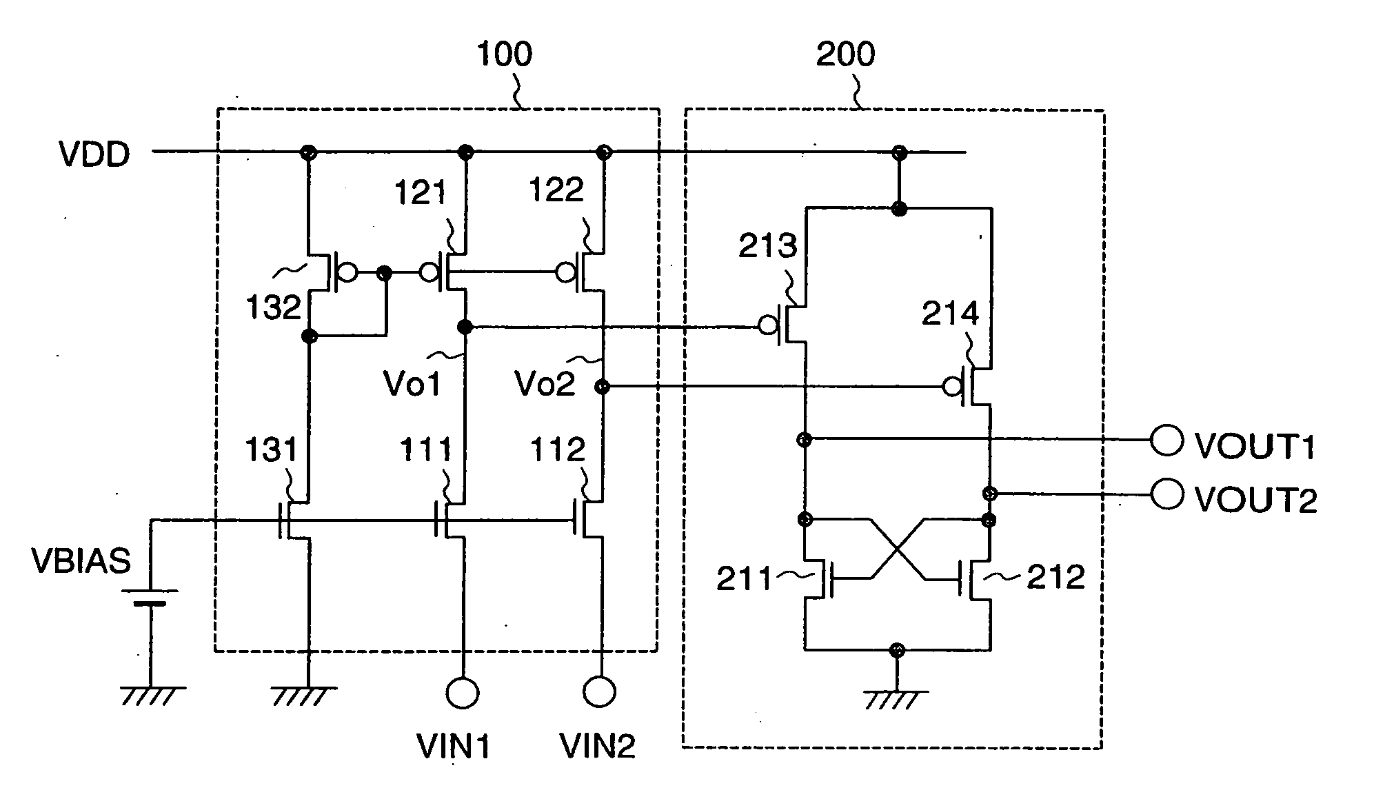
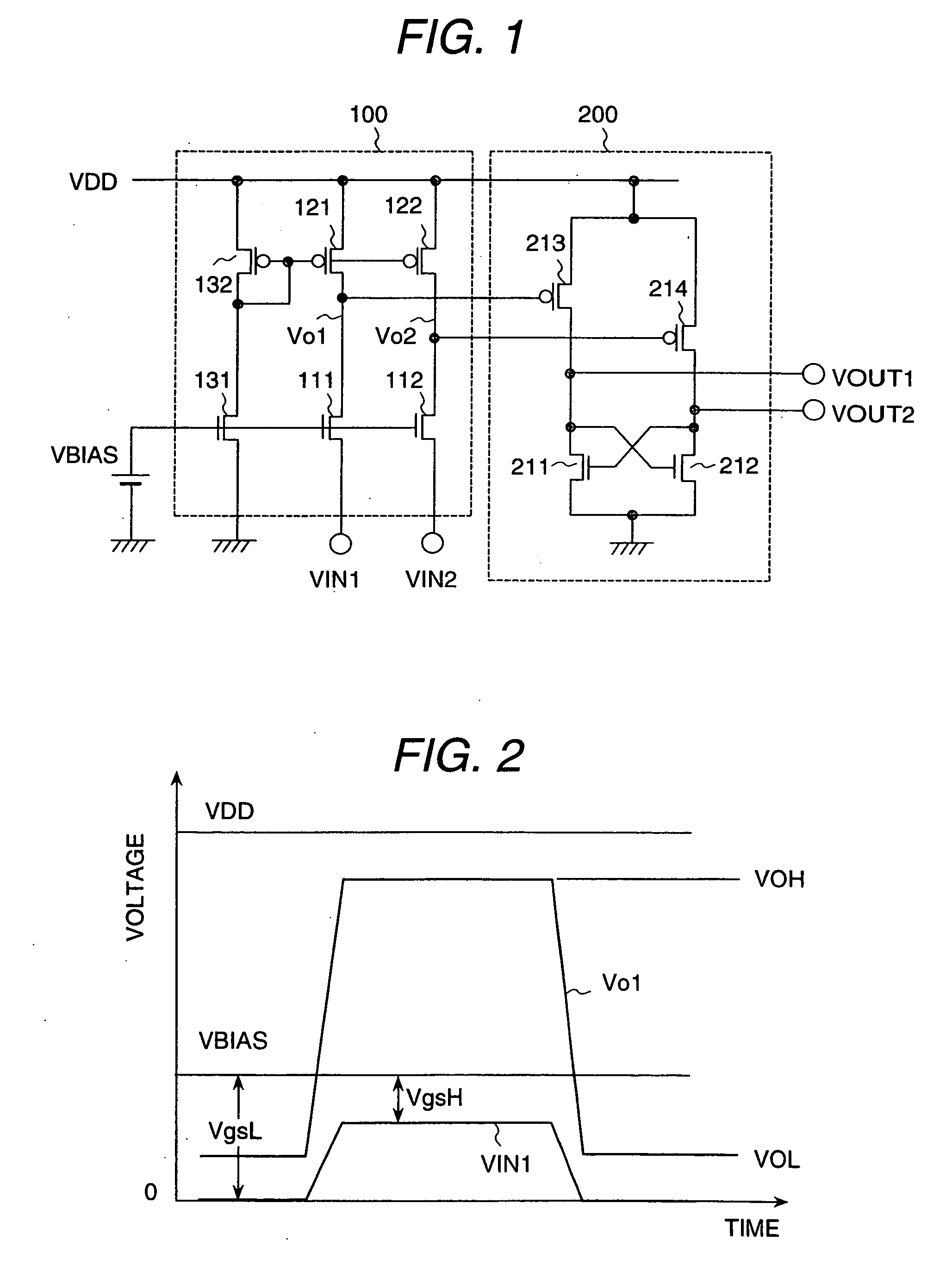
[0039]FIG. 1 shows a level conversion circuit in a liquid crystal display apparatus forming a first embodiment according to the present invention. The level conversion circuit is constituted by a level conversion unit 100 and a wave-form shaping unit 200.

[0040] The level conversion unit 100 is constituted by input transistors 111 and 112, load transistors 121 and 122, and bias transistors 131 and 132. In the level conversion unit 100, a respective gate electrode of the respective input transistors 111 and 112 is connected to a bias power supply VBIAS, a respective source electrode of the respective input transistors 111 and 112 is connected to input terminals VIN1 and VIN2, and a respective drain electrode of the respective input transistors 111 and 112 is connected to outputs Vo1 and Vo2, respectively.

[0041] In the level conversion unit 100, the gate electrodes of the respective load transistors 121 and 122 are connected in common to the bias use transistor 132, the source electro...

second embodiment

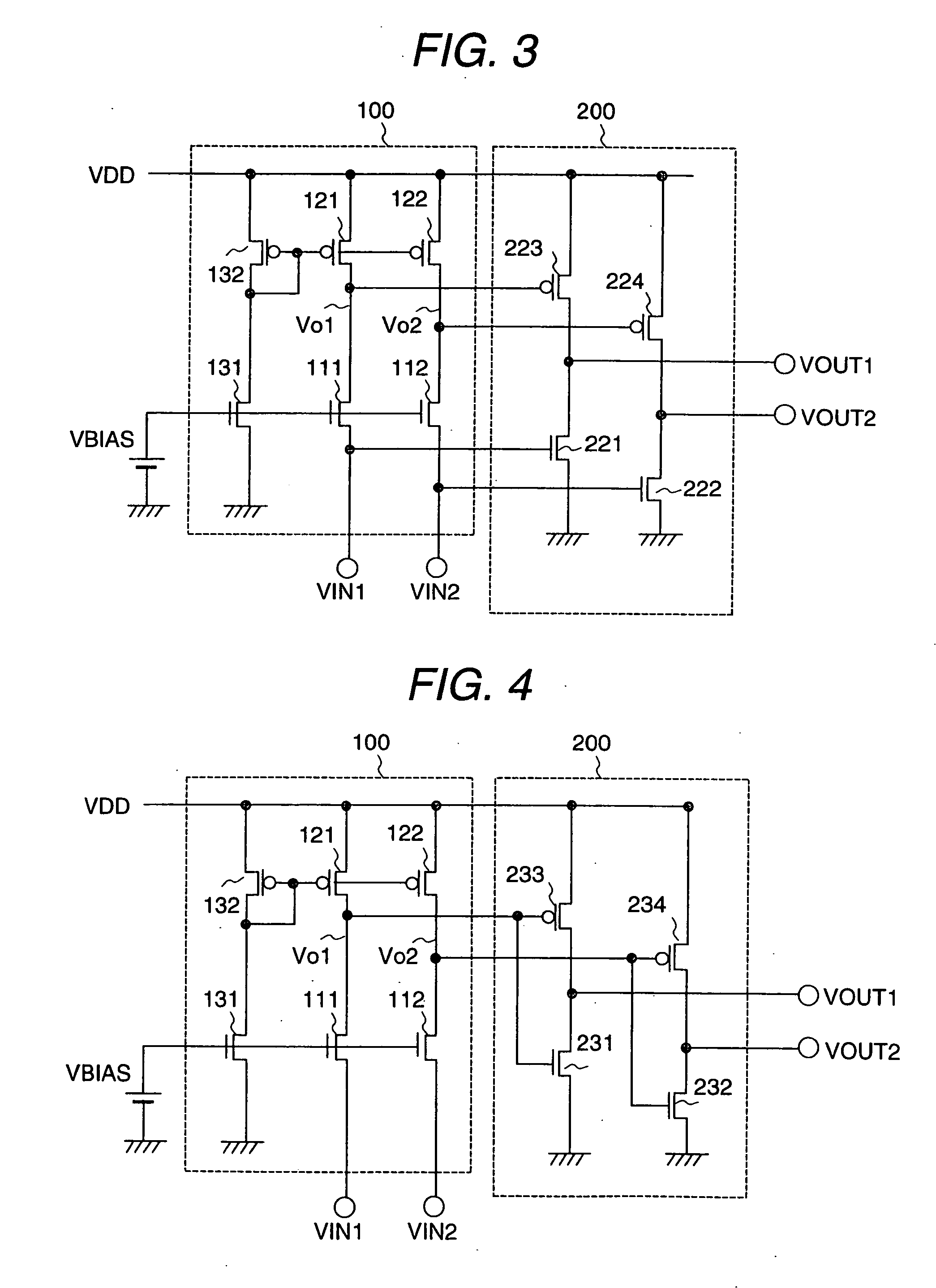
[0057]FIG. 3 shows a level conversion circuit in a liquid crystal display apparatus representing a second embodiment according to the present invention. This second embodiment according to the present invention differs from the first embodiment shown in FIG. 1, and the difference is in the wave-form shaping unit 200 shown in FIG. 3.

[0058] The wave-form shaping unit 200 of this second embodiment according to the present invention is constituted of N-type load transistors 221 and 222 and P-type input transistors 223 and 224. The respective source electrodes of the N-type load transistors 221 and 222 are grounded, the respective gate electrodes of the load transistors 221 and 222 are connected to the input terminals VIN1 and VIN2, and the respective drain electrodes of the load transistors 221 and 222 are connected to the respective drain electrodes of the P-type input transistors 223 and 224, respectively.

[0059] The respective source electrodes of the P-type input transistors 223 and...

third embodiment

[0064]FIG. 4 shows a level conversion circuit in a liquid crystal display apparatus representing a third embodiment according to the present invention. This third embodiment differs from the first embodiment shown in FIG. 1, and the difference is in the wave-form shaping unit 200.

[0065] The wave-form shaping unit 200 of this third embodiment according to the present invention is constituted of N-type load transistors 231 and 232 and P-type input transistors 233 and 234. Each of the N-type load transistor 231 and the P-type input transistor 233 and each of the N-type load transistor 232 and the P-type input transistor 234 constitutes, respectively, an inverter circuit.

[0066] The operation of the wave-form shaping unit 200 constituted as described above will be explained. As one example of the conditions of operation, the voltages of the input terminals VIN1 and VIN2 are respectively 3.3 V and 0 V, the voltage of the power supply VDD is 15 V and the voltage of the bias power supply i...


PUM

PropertyMeasurementUnit
voltage amplitudeaaaaaaaaaa

Abstract

A liquid crystal display apparatus having a level conversion circuit in which a high speed operation can be attained and also a small transistor capacity can be obtained is provided. In the liquid crystal display apparatus, a signal circuit for driving pixel elements of a display unit and a scanning circuit are provided. The level conversion circuit is constituted of a first and a second transistors 111 and 112 in which a respective gate electrodes is connected to a first bias voltage power supply, and a third and a fourth transistors 121 and 122 in which a respective gate electrodes is connected to a second bias voltage power supply and a respective source electrodes is connected to a power supply.

Description

CROSS-REFERENCE TO RELATED APPLICATIONS [0001] This is a continuation of application Ser. No. 10 / 797,013 filed 11 Mar. 2004, allowed, which is a continuation of application Ser. No. 10 / 150,952 filed 21 May 2002 and issued as U.S. Pat. No. 6,714,184 B2, which is a continuation of application Ser. No. 09 / 337,260 filed 22 Jun. 1999 and issued as U.S. Pat. No. 6,392,625 B1, the contents of all of which are incorporated herein by reference in their entirety.BACKGROUND OF THE INVENTION [0002] The present invention relates to a liquid crystal display apparatus having a level conversion circuit in which a signal having a low voltage amplitude is converted to a signal having a high voltage amplitude; and, in particular, the invention relates to a level conversion circuit for use in a clock interface and a data interface of a liquid crystal display apparatus using thin-film transistors (TFT: Thin-Film Transistor). [0003] A level conversion circuit of the type used in a clock interface and a d...

Claims


Application Information

Patent Timeline
Patent Type & Authority Applications(United States)
IPC IPC(8): G09G5/00G09G3/36G02F1/133H03K3/356H03K19/0185
CPCG09G3/3611G09G3/3674G09G3/3685H03K19/018521G09G2310/0289H03K3/356147G09G5/006B31B50/14B31B2120/30
Inventor SATO, HIDEOMIKAMI, YOSHIROKAGEYAMA, HIROSHIOHKUBO, TATSUYA
Owner PANASONIC LIQUID CRYSTAL DISPLAY CO LTD
Why Eureka
Try Eureka