Semiconductor device and method of manufacturing the same

a technology of semiconductors and semiconductors, applied in the direction of semiconductor devices, electrical devices, transistors, etc., can solve the problems of deteriorating refresh operation, affecting varying the height of potential barriers near the source, so as to improve the refresh operation of memory cells, prevent punching, and prevent the effect of punching

Inactive Publication Date: 2006-01-12
SAMSUNG ELECTRONICS CO LTD
View PDF29 Cites 3 Cited by
  • Summary
  • Abstract
  • Description
  • Claims
  • Application Information

AI Technical Summary

Benefits of technology

[0017] Embodiments of the invention solve the aforementioned problems. Some embodiments of the invention provide a semiconductor device capable of preventing punchthrough between the source and drain regions of a transistor, while also improving the refresh operation of a memory cell. Other embodiments of the invention provide a method for manufacturing a semiconductor device capable of preventing punchthrough between the source and drain regions of a transistor while also improving the refresh operation of a memory cell. Embodiments of the invention can be applied to all types of PMOS and NMOS devices.

Problems solved by technology

In addition to a decreased threshold voltage, punchthrough between the source and drain regions is another severe problem accompanying the short channel effect.
However, the surface of the substrate is depleted to some degree by the gate electrode, thereby varying the height of the potential barrier near the source.
This results in the deterioration of the refresh operation.
Accordingly, a large electric field is applied to the region where the n-type source and drain regions and the p-type channel region make contact with each other, generating an increased junction leakage current and a deterioration of the refresh operation.
The method of forming the partition by filling the interior of the insulator with a conductor can prevent this problem, but the required manufacturing process is complicated.

Method used


Image

  • Semiconductor device and method of manufacturing the same
  • Semiconductor device and method of manufacturing the same
  • Semiconductor device and method of manufacturing the same

Examples


Embodiment Construction

[0027] Hereinafter, embodiments of the invention will be described in detail with reference to the accompanying drawings. In the following drawings, the same numerals indicate the same elements.

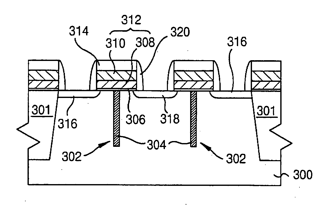
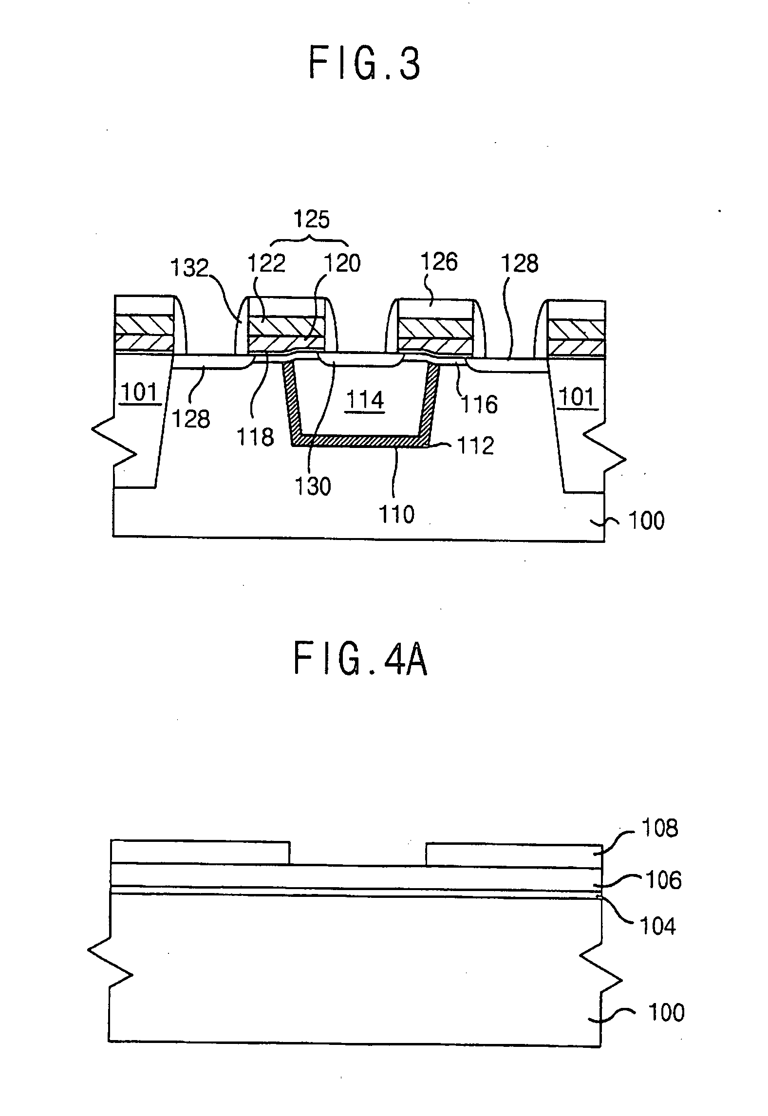
[0028]FIG. 2 is a plane view showing a memory cell of a semiconductor device in accordance with an embodiment of the invention. FIG. 3 is a cross-sectional view of the memory cell, taken along the line A-A′ of the FIG. 2.

[0029] Referring to FIGS. 2 and 3, a trench 110 is formed in an active region 102 of a semiconductor substrate 100 divided into an isolation region 101 and the active region 102. Preferably, the trench 110 is formed to have a width (w) wider than that of the active region 102. Although the isolation region 101 is formed to have a shallow trench isolation structure in the embodiment of FIG.3, the isolation region 101 may be formed to have a LOCOS-type structure without limiting the present invention.

[0030] A doped layer 112 for adjusting a threshold voltage and preventing p...


PUM


Abstract

A semiconductor device and a method of manufacturing the same is disclosed. A trench is formed in an active region of a semiconductor substrate. A doped layer is formed on the inner walls of the trench. The trench is filled up with a first semiconductor layer. A gate insulating layer is formed on the first semiconductor layer and the substrate. Two gate electrodes are formed on the gate insulating layer such that the trench is located in between two gate electrodes. First and second impurity regions are formed in the substrate on both sides of each of the gate electrodes. Since the doped layer is locally formed in the trench area, the source and drain regions are completely separated from the heavily doped layer to weaken the electric field of PN junction, thereby improving refresh and preventing punchthrough between the source and drain.

Description

CROSS REFERENCE TO RELATED APPLICATIONS [0001] This is a Divisional of U.S. patent application Ser. No. 10 / 445,109, filed on May 23, 2003, now pending, which claims priority from Korean Patent Application No. 2002-38708, filed on Jul. 4, 2002, which is incorporated by reference in is entirety.BACKGROUND OF THE INVENTION [0002] 1. Field of the Invention [0003] This disclosure relates to a semiconductor device and a method of manufacturing the same. More particularly, the disclosure relates to a semiconductor device capable of preventing the “punchthrough” phenomenon between source and drain regions of a transistor, improving the refresh characteristics of a memory cell, and a method of manufacturing the same. [0004] 2. Description of the Related Art [0005]FIG. 1 is a cross-sectional view of a conventional MOS transistor. Referring to FIG. 1, the MOS transistor comprises a gate electrode 3 stacked on a semiconductor substrate 1 with a gate oxide layer 2 interposed between them, with s...

Claims


Application Information

Patent Timeline
Patent Type & Authority Applications(United States)
IPC IPC(8): H01L21/336H01L21/8234H01L29/423H01L21/8242H01L27/088H01L27/108H01L29/10H01L29/49H01L29/78
CPCH01L27/10873H01L29/1041H01L29/1045H01L29/105H01L29/78H01L29/66537H01L29/66553H01L29/66651H01L29/1083H10B12/05
Inventor SON, NAK-JINKIM, JI-YOUNG
Owner SAMSUNG ELECTRONICS CO LTD
Why Eureka
Try Eureka