Memory Structures for Expanding a Second Bit Operation Window

a memory operation and second bit technology, applied in the field of memory operation windows, can solve the problems of large vt distribution of erase state, difficult to erase, and charge loss in the high threshold cell and charge gain in the low threshold cell, and achieve the effect of increasing the memory operation window and reducing the second bit

Active Publication Date: 2007-12-27
MACRONIX INT CO LTD
View PDF15 Cites 3 Cited by
  • Summary
  • Abstract
  • Description
  • Claims
  • Application Information

AI Technical Summary

Benefits of technology

[0018]Advantageously, the present invention provides methods and structures for increasing a memory operation window in a charge trapping memory and reducing the second bit effect. The present invention is also applicable to low voltage memory applications.

Problems solved by technology

However, the hot hole injection causes oxide damage, leading to charge loss in the high threshold cell and charge gain in the low threshold cell.
This difference in erase speed results in a large Vt distribution of the erase state, where some of the cells become hard to erase and some of them are over-erased.
Thus the target threshold Vt window is closed after many program and erase cycles and poor endurance is observed.
This phenomenon will become more serious when the technology keeps scaling down.

Method used


Image

  • Memory Structures for Expanding a Second Bit Operation Window
  • Memory Structures for Expanding a Second Bit Operation Window
  • Memory Structures for Expanding a Second Bit Operation Window

Examples


first embodiment

[0063]Turning now to FIG. 2, there is shown a structural diagram illustrating an erase method by employing a hole tunneling erase of the SONOS memory 200 to a negative voltage threshold by applying a positive gate voltage from a gate terminal of the SONOS memory 200. The SONOS memory 200 comprises a charge trapping structure 212 overlaying a first dielectric layer 210, and a second dielectric layer 214 overlaying the charge trapping structure 212. An n-poly layer 220 overlies the second dielectric layer 214. A high bias voltage applied at a gate terminal causes a band distortion so that the second dielectric layer 214 may be thinner at certain regions to allow holes to penetrate through the second dielectric layer 214. When a high bias voltage is applied to a gate terminal in the n-poly 220, holes are injected from the gate terminal (as indicated by arrows 240a, 240b), through the second dielectric layer 214, and to the charge trapping structure 212. The second dielectric layer 214 ...

second embodiment

[0064]In FIG. 3, there is shown a structural diagram illustrating the erase method by applying a hole tunneling erase to a SONOS memory cell 300 to bring the memory cell to a negative voltage threshold by applying a negative gate voltage from a substrate of a SONOS memory cell 300. The SONOS memory cell 300 comprises a charge trapping structure 312 overlaying a first dielectric layer 310, and a second dielectric layer 314 overlaying the charge trapping structure 312. An n-poly layer 320 overlies the second dielectric layer 314. A high negative bias voltage applied at a substrate 302 causes a band distortion so that the first dielectric layer 310 may be thinner at certain regions to allow holes to penetrate through first dielectric layer 310. When a high negative bias voltage is applied to the substrate 302, holes are injected from the substrate 302 (as indicated by arrows 340a, 340b), through the first dielectric layer 310, and to the charge trapping structure 312. The first dielect...

third embodiment

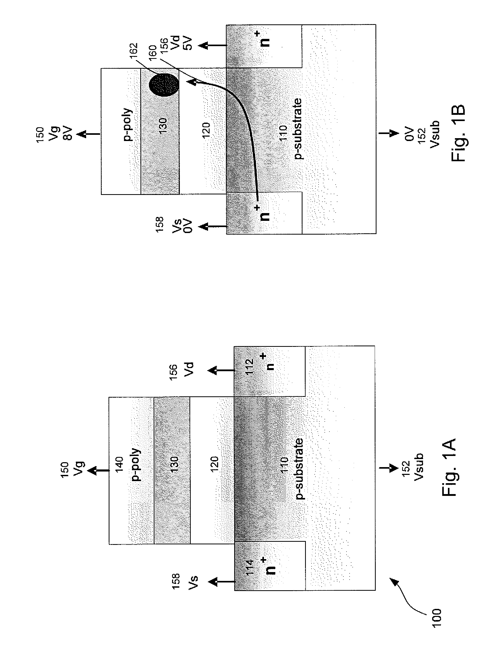
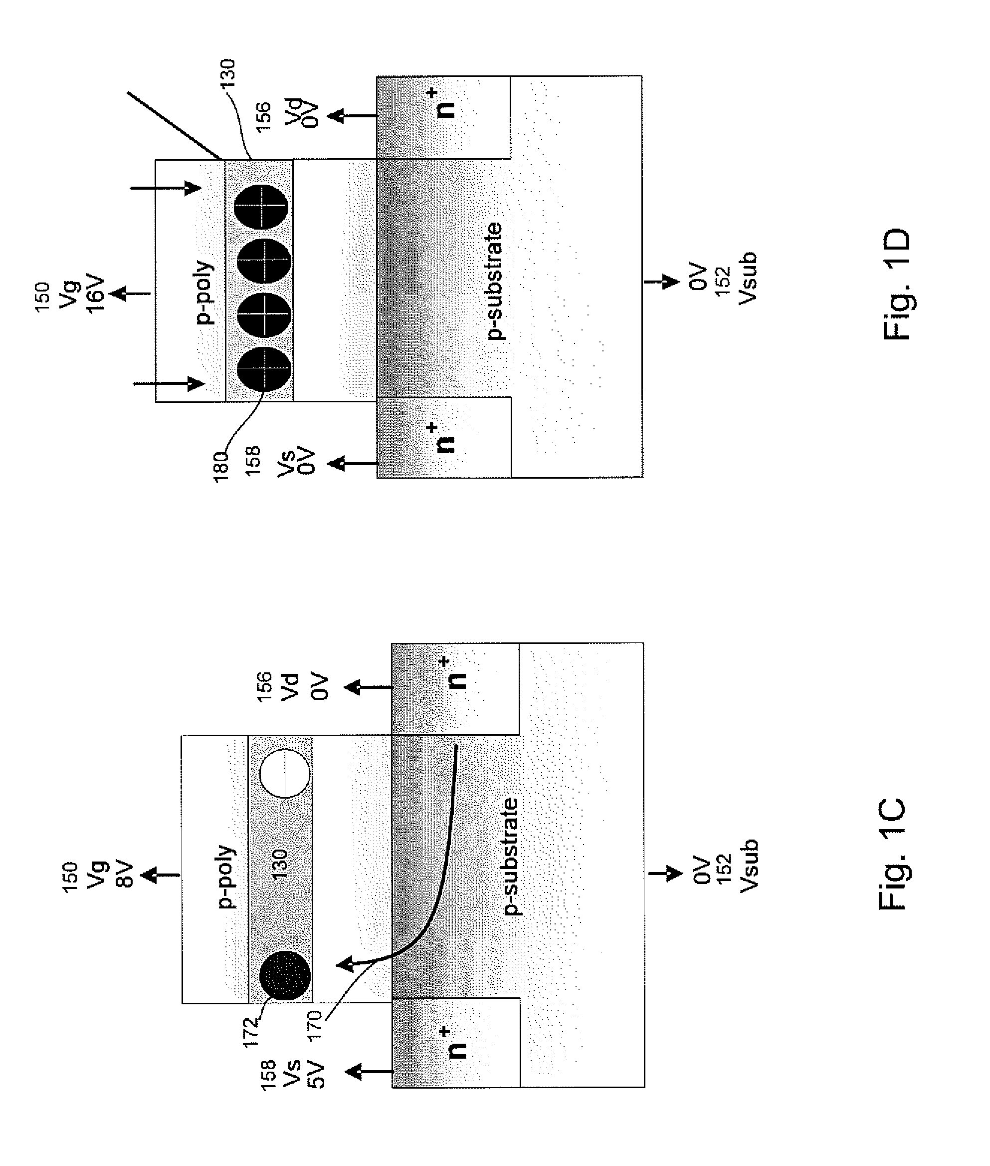
[0065]FIGS. 4A-4B are structural diagrams illustrating the erase method by employing a band-to-band hot hole erase to a negative voltage threshold in the SONOS memory cell 300. The erase operation of a right bit in the SONOS memory cell 300 is illustrated in FIG. 4A and the erase operation of a left bit in the SONOS memory cell 300 is illustrated in FIG. 4B. When erasing a right bit using a band-to-band hot hole erase, a drain voltage Vd 434 is applied with 5 volts and a source voltage Vs 436 is applied with 0 volts in order to move holes toward the right side of a charge trapping structure 410, as indicated by an arrow 420. The bias voltage conditions are reversed in erasing a left bit. When erasing a left bit using a band-to-band hot hole erase, the source voltage Vs 436 is applied with 5 volts and the drain voltage Vd 434 is applied with 0 volts, as indicated by an arrow 422. In both erase operations of the right bit and the left bit, a gate voltage Vg 430 is applied with 8 volts...


PUM


Abstract

Methods and structures are described for increasing a memory operation window in a charge trapping memory having a plurality of memory cells in which each memory cell is capable of storing multiple bits per memory cell. In a first aspect of the invention, a first method to increase a memory operation window in a two-bit-per-cell memory is described by applying a positive gate voltage, +Vg, to erase a memory cell to a negative voltage level. Alternatively, a negative gate voltage, −Vg, is applied to the two-bit-per-cell memory for erasing the memory cell to a negative voltage level. A second method to increase a memory operation window is to erase a memory cell to a voltage level that is lower than an initial voltage threshold level. These two erasing methods can be implemented either before a programming step (i.e., a pre-program erase operation) or after a programming step (i.e., a post-program erase operation).

Description

CROSS REFERENCE TO RELATED APPLICATIONS[0001]This application relates to a concurrently filed and co-pending U.S. patent application Ser. No. ______, entitled “Methods and Structures for Expanding a Memory Operation Window and Reducing a Second Bit Effect” by Chao-I Wu, owned by the assignee of this application and incorporated herein by reference.[0002]This application relates to a concurrently filed and co-pending U.S. patent application Ser. No. ______, entitled “Top Dielectric Structures in Memory Devices and Methods for Expanding a Second Bit Operation Window” by Chao-I Wu, owned by the assignee of this application and incorporated herein by reference.[0003]This application relates to a concurrently filed and co-pending U.S. patent application Ser. No. ______, entitled “Bottom Dielectric Structures and High-K Memory Structures in Memory Devices and Methods for Expanding a Second Bit Operation Window” by Chao-I Wu, owned by the assignee of this application and incorporated herei...

Claims


Application Information

Patent Timeline
Patent Type & Authority Applications(United States)
IPC IPC(8): G11C16/04
CPCG11C16/0475H01L29/7923H01L29/517H01L29/513
Inventor WU, CHAO-I
Owner MACRONIX INT CO LTD
Why Eureka
Try Eureka