Programmable spatial filter for wafer inspection

Inactive Publication Date: 2006-01-19
NEGEVTECH
View PDF90 Cites 55 Cited by
  • Summary
  • Abstract
  • Description
  • Claims
  • Application Information

AI Technical Summary

Benefits of technology

[0021] According to a further preferred embodiment of the present invention, there is provided a novel, double layer SLM, in which the fill factor is increased in comparison to a single layer SLM using the same devices. The SLM arrays of this double SLM array are essentially identical, and are arranged one on top of the other and in close proximity, such that the light to be spatially modulated has to pass serially through both of the individual arrays. The double SLM array relies for its operation on the asymmetric placement of the dead area within each pixel. Two conditions are necessary for the correct operation of the double layered SLM embodiment of the present invention. Firstly, the individual arrays are laterally positioned such that their dead areas are collinearly located in relation to the light transmission through the array. Secondly, th

Problems solved by technology

However, many LCD materials do not stand up well to the UV illumination used in wafer inspection systems.
However, the use of any LCD array, regardless of the materials used, generally results in a limited transmission level in the regions which are switched to the “open” or transparent state, and a limited blocking level in the regions which are switched to the “closed” or opaque state.
Additionally, changes i

Method used


Image

  • Programmable spatial filter for wafer inspection
  • Programmable spatial filter for wafer inspection
  • Programmable spatial filter for wafer inspection

Examples


Embodiment Construction

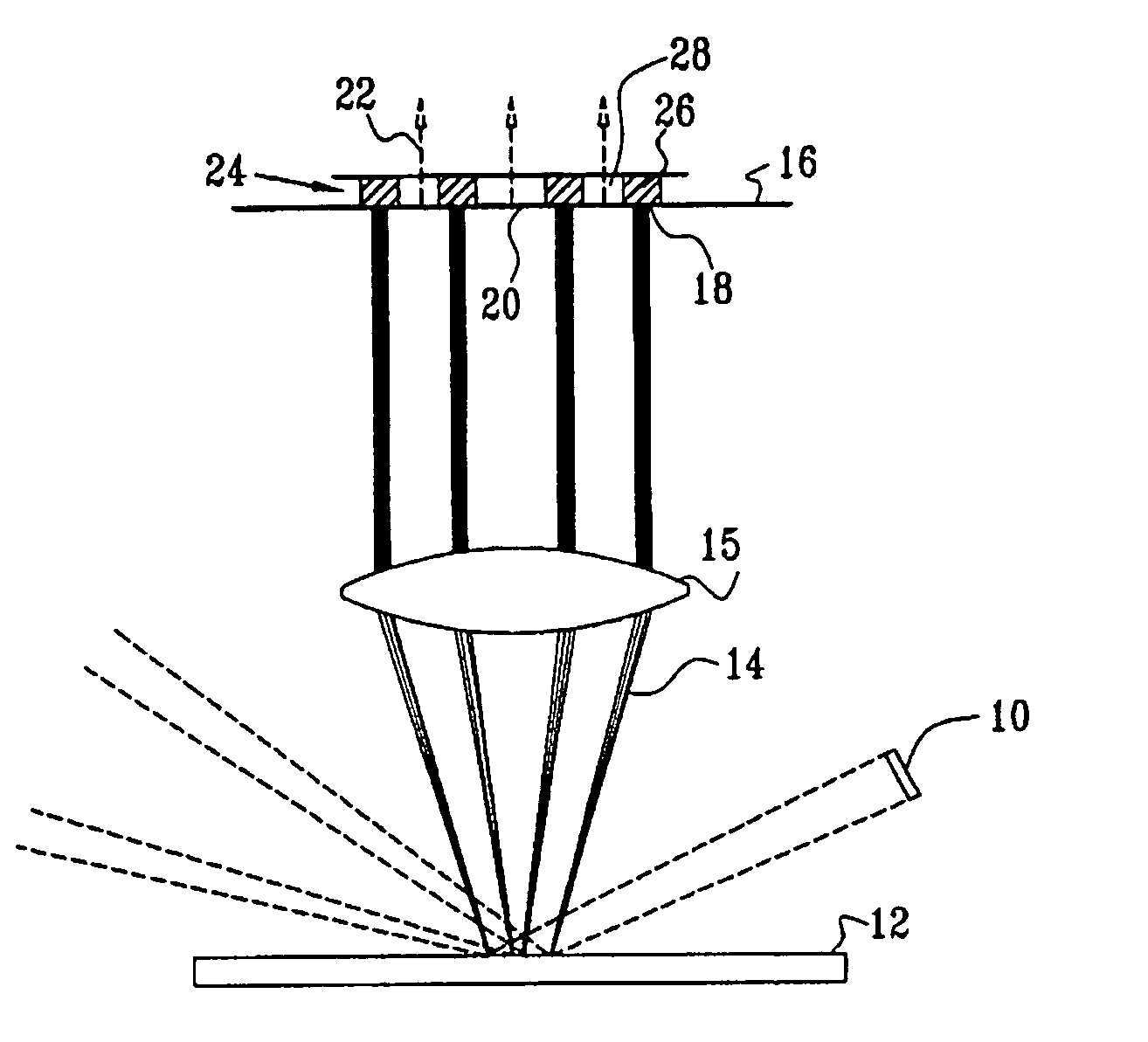
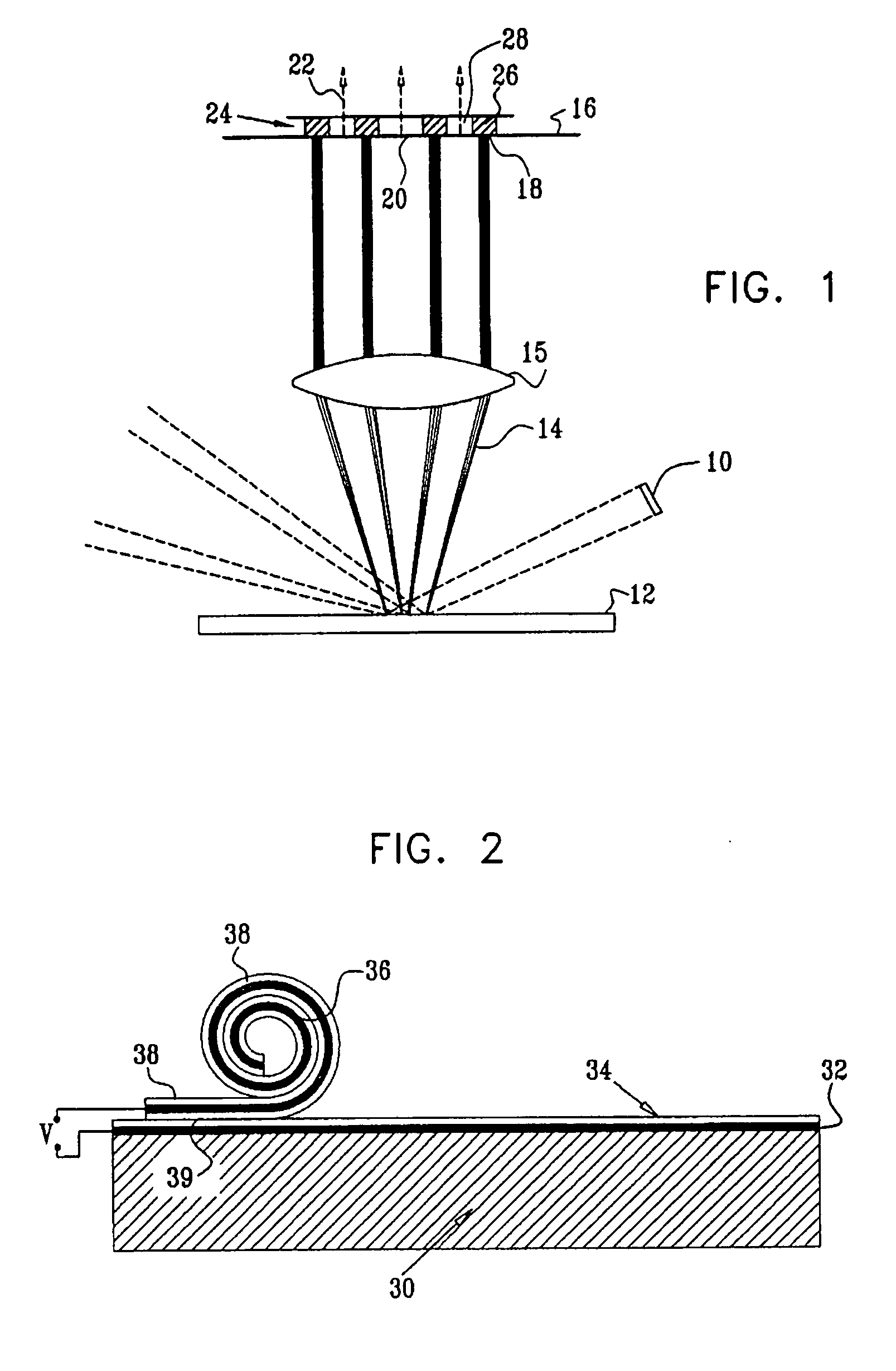
[0044] Reference is now made to FIG. 1, which illustrates schematically the dark field illumination system of a wafer inspection system utilizing a MEMS Fourier plane filter, according to a first preferred embodiment of the present invention. The light source 10, which can be non-parallel, is incident on the wafer 12 under inspection. The scattered light 14 from the wafer features is imaged by the objective lens 15. At the back focal plane 16 of this lens, which is the Fourier plane, there is generated a patterned array of spots 18 representing the repetitive features of the wafer being imaged by the scattered light. In the interstitial positions 20 between these spots, there may appear any light scattered from non-repetitive features on the wafer die, such as from a defect which it is desired to detect. A mask 24, preferably comprising a spatial light modulator (SLM) preferably made up of an array of MEMS shutters, is disposed at the Fourier plane 16. The individual MEMS elements o...


PUM


Abstract

A programmable spatial filter for use as a Fourier plane filter in dark field wafer inspection systems, based on the use of MEMS (Micro-Electro-Mechanical Systems) devices. In comparison with prior art systems, especially those using LCD's, the use of MEMS devices provide a number of potential advantages, including good transmission in the UV, a high fill factor, polarization independence and a high extinction ratio since the shutter is opaque when closed. The MEMS devices can be flap devices, artificial eyelid, or double shutter devices. Additionally, a novel spatial light modulator (SLM) assembly having a double layer of SLM arrays is described, in which the fill factor is increased in comparison to a single layer SLM using the same devices, by positioning the dead areas of the elements of both arrays collinearly in the modulated beam. This SLM assembly can be implemented using pixelated LCD arrays or MEMS arrays.

Description

FIELD OF THE INVENTION [0001] The present invention relates to the field of the use of programmable spatial filters based on the use of MEMS devices, especially for use as a Fourier plane filter in the imaging system of a wafer inspection system. BACKGROUND OF THE INVENTION [0002] Wafer inspection systems are used in the semiconductor industry for the detection of small defects and anomalies occurring within the chips on the wafers, generally arising during the fabrication process. The geometry on a semiconductor wafer generally consists of a large-scale multiply repetitive pattern that defines the dies of the wafer. Within each die, there are often areas in which there appears an array of a repetitive pattern with a cycle of a few microns or less. This occurs especially in memory chips or in the memory area in a logic chip. The inspection system should be capable of detecting even defects occurring within these repetitive regions. [0003] When coherent or partially coherent illumina...

Claims


Application Information

Patent Timeline
IPC IPC(8): G01N21/88
CPCG01N21/9501G01N2201/0675G01N2021/8822G01N21/95623
Inventor FRADKIN, KERENDOTAN, NOAM
Owner NEGEVTECH
Why Eureka
Try Eureka