Unlock instant, AI-driven research and patent intelligence for your innovation.

Exposure apparatus and semiconductor device manufacturing method

a technology of semiconductor devices and manufacturing methods, applied in the direction of shock absorbers, instruments, printing, etc., can solve the problems of adversely affecting the performance of the stage device as well as that of the optical system and measurement system, and it is difficult to arrange two stage devices having completely the same specifications. , to achieve the effect of reducing the influence, suppressing the vibration of the base, and reducing the vibration

Inactive Publication Date: 2006-01-26
CANON KK
View PDF8 Cites 40 Cited by
  • Summary
  • Abstract
  • Description
  • Claims
  • Application Information

AI Technical Summary

Benefits of technology

The present invention aims to provide an apparatus and method that can reduce the impact of a stage device in a base where it is mounted, which cannot be effectively canceled out by a counter mass system. This invention can help decrease and suppress vibration of the base, resulting in improved accuracy and efficiency in the manufacturing process of semiconductor devices.

Problems solved by technology

This is because when vibration occurs in a structure that forms an exposure stage or exposure apparatus main body, it adversely affects exposure.
This is because if vibration occurs in the exposure apparatus main body, it adversely affects the performance of the stage device as well as that of an optical system and measurement system which are mounted on the same base and vibration-damping bed where the stage device is mounted.
In actual design and application of an apparatus, it is very difficult to arrange two stage devices having completely the same specifications such that their axes in which driving reaction forces occur coincide with each other completely.
This is because very often the arrangement and design of the unit are spatially limited.
Consequently, vibration occurs in the base.
In practice, the stage device and counter masses are structures having comparatively large weights, and accordingly it is difficult to obtain their masses sufficiently accurately and to reflect them in the control operation.
If parameter adjustment is not performed sufficiently accurately, the counter mass system does not operate appropriately, and a thrust acts on the base to vibrate it.

Method used


Image

  • Exposure apparatus and semiconductor device manufacturing method
  • Exposure apparatus and semiconductor device manufacturing method
  • Exposure apparatus and semiconductor device manufacturing method

Examples


first embodiment

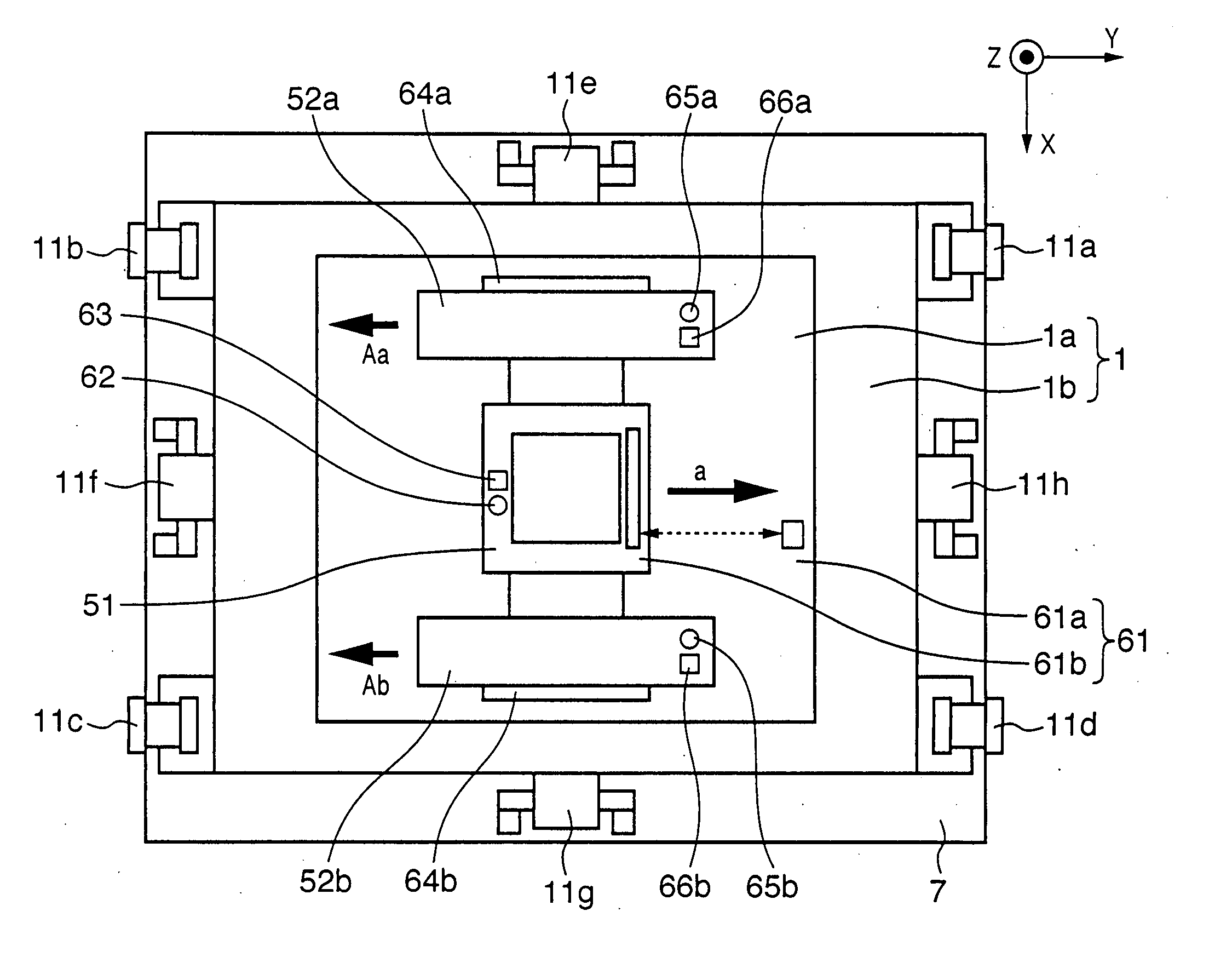
[0051]FIGS. 1 and 2 are views for explaining the structure and operation of a unit around a stage device that forms an exposure apparatus according to the first preferred embodiment of the present invention. FIGS. 1 and 2 show a stage device having a kinetic freedom in the direction of one degree of freedom. FIG. 1 is a plan view of the exposure apparatus, and FIG. 2 is a side view of the exposure apparatus. This unit corresponds to the reticle stage device 95 in the exposure apparatus shown in FIG. 7.

[0052] In this manner, the reticle stage device 95 is a stage device which has one degree of kinetic freedom. Actually, the stage device sometimes has not only one degree of freedom in a Y direction shown in FIG. 1 but also a kinetic freedom in X, θz, or the like for reticle alignment. Note that a comparatively large driving reaction force is generated in one degree of freedom, i.e., in the Y direction in which the reticle stage device 95 is scanned.

[0053] As the substrate stage devi...

second embodiment

[0099] In the first embodiment, the stage device operates in the direction of one degree of freedom. This stage device corresponds to the reticle stage device 95 in the exposure apparatus described with reference to FIG. 7. The structure of the present invention can also be applied to a stage device, e.g., a substrate stage, which moves in the directions of two degrees of freedom. In a stage system including a stage device which operates in the directions of two degrees freedom and counter masses configured to cancel the driving reaction force of the stage device, a device will be described in which a thrust and moment which are not completely canceled by the mutual operations of the stage device and counter masses but transmitted to a base where the stage device and counter masses are mounted are estimated, and actuators which apply a control force to the base are controlled on the basis of estimation signals to decrease and suppress the vibration of the base.

[0100]FIGS. 4 and 5 a...

third embodiment

[0146] The first and second embodiments exemplify an apparatus and structure for controlling the actuators which apply a control force to the base on the basis of the motion physical values, e.g., the position information (displacement), velocity information, and acceleration information of the stage device and counter masses. Equations (1) to (4) will be reviewed. For the sake of simplicity, equation (1) will be discussed.

[0147] According to the basic operation of a stage device, e.g., the stage device described in the present invention which includes counter masses, the motion physical values, e.g., position (displacement), velocity, and acceleration are transferred between the stage device and counter masses. Forces from the stage device and counter masses do not act on the base or the like where the stage device and counter masses are mounted. Considering this point, in an ideal state, for example, if the relationship of equation (5) is maintained, fy and Mqz in the left member...


PUM


Abstract

An exposure apparatus includes a base, a stage device which is mounted on the base and moves in a predetermined direction, a counter mass which is mounted on the base and moves in a direction opposite to the predetermined direction as the stage device moves, a sensor which detects a motion physical value of each of the stage device and counter mass, and an actuator which applies a force to the base on the basis of a detection result of the sensor.

Description

FIELD OF THE INVENTION [0001] The present invention relates to an exposure apparatus and a semiconductor device manufacturing method which utilizes the same and, more particularly, to an exposure apparatus having a mechanism which effectively suppresses vibration generated by driving a stage device, and a semiconductor device manufacturing method which utilizes the exposure apparatus. BACKGROUND OF THE INVENTION [0002] As the accuracy of a semiconductor exposure apparatus increases, a higher-performance vibration-damping, vibration control technique is sought for. This is because when vibration occurs in a structure that forms an exposure stage or exposure apparatus main body, it adversely affects exposure. Therefore, a technique is required which insulates the exposure apparatus main body from vibration outside the exposure apparatus, e.g., from an apparatus installation pedestal, and effectively and quickly decreases vibration generated by the operation of a device which includes ...

Claims


Application Information

Patent Timeline
Patent Type & Authority Applications(United States)
IPC IPC(8): G03B27/58
CPCF16F7/1005G03F7/70766G03F7/70716F16F15/02G03F7/70758
Inventor MAYAMA, TAKEHIKO
Owner CANON KK