Process for obtaining spatially-organised nanostructures on thin films

a nanostructure and nano-structure technology, applied in the field of spatially-organised nanostructures on thin films, can solve the problems of inability to erase dots, inability to achieve straightforward technological use, and excessive slowness of single probe spm, and achieve the effect of high areal density of dots

Inactive Publication Date: 2006-01-26
SCRIBA NANOTECNOLOGIE SRL
View PDF6 Cites 1 Cited by
  • Summary
  • Abstract
  • Description
  • Claims
  • Application Information

AI Technical Summary

Benefits of technology

[0009] Another aim of the present invention is to provide a process that makes possible to generate, simultaneously, an arbitrary number of dots, from 1 to as many dots are desired, organised into strings along well-defined lines on a thin film deposited on a substrate, the dots having the same size and being periodically spaced.
[0010] Still another aim of the present invention is that of providing a process for forming nanostructures that is scalable and allows to obtain high areal density of dots.
[0011] A further aim of

Problems solved by technology

This density is however accessible only on perfect crystal surfaces in ultra-high vacuum, which are of no straightforward technological use.
Moreover, a single probe SPM is excessively slow, with best data rates demonstrated of 100 kbit/s in writing, and 1-10 Mbit/s for reading.
[12] The millipede technology has also some drawbacks

Method used


Image

  • Process for obtaining spatially-organised nanostructures on thin films
  • Process for obtaining spatially-organised nanostructures on thin films
  • Process for obtaining spatially-organised nanostructures on thin films

Examples


Embodiment Construction

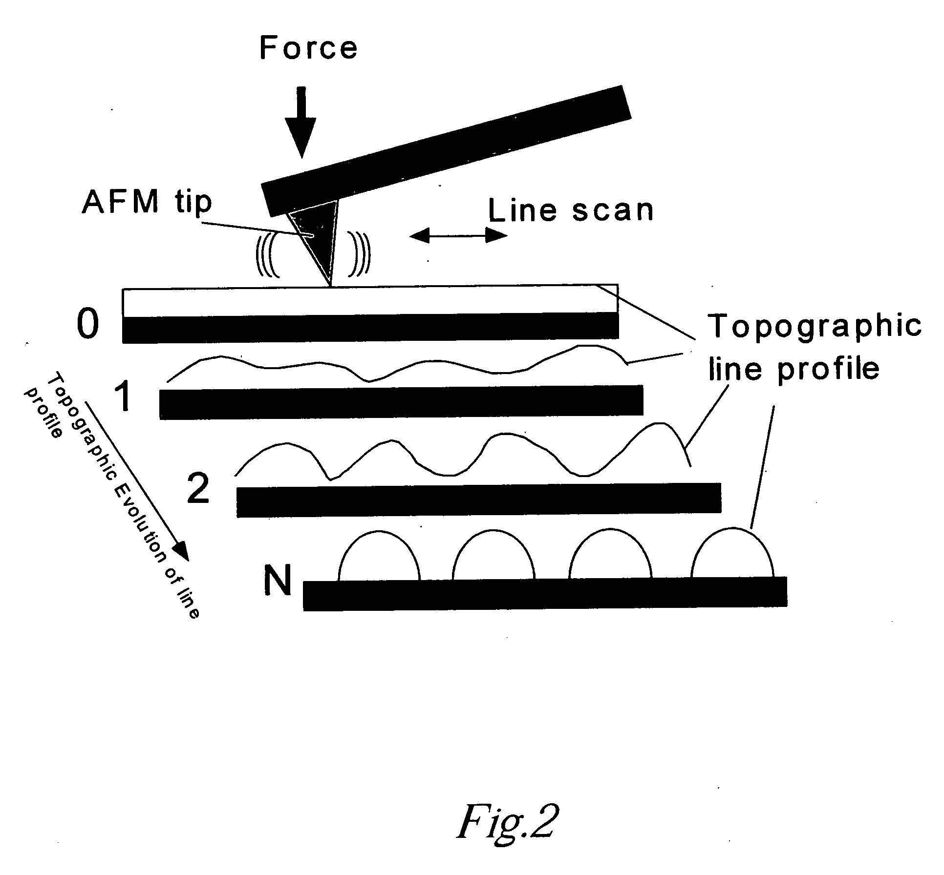
[0028] The present invention regards a new process that allows the formation of nanostructures by self-organization of bistable molecules, starting from an initially smooth and featureless thin film. The nanostructures are formed only when a local external perturbation, of well defined intensity, is applied. The nanostructures can be controlled and preset in number, size, distance, form. Such nanostructures with the said characteristics can be used to store information or other usages that will become clear in the following.

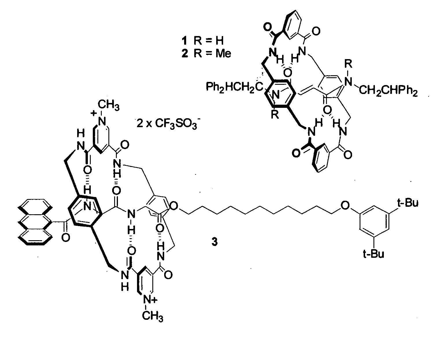
[0029] Storage information media can be obtained with the process of the present invention by obtaining of a thin film of bistable molecules, preferably taken from the class of rotaxanes. Rotaxanes consist of a molecular macrocycle locked around a molecular thread, that has two bulky groups, the stoppers, at both ends to prevent the macrocycle from slipping off the thread.

[0030] Examples of rotaxanes used to demonstrate the process are illustrated in the scheme...


PUM

PropertyMeasurementUnit
Lengthaaaaaaaaaa
Thicknessaaaaaaaaaa
Forceaaaaaaaaaa

Abstract

A process for forming nanostructures comprising the step of applying on localised regions of a smooth thin film of bistable or multistable molecules an external perturbation with preset magnitude thereby said film undergoes a collective morphological transformation and nanostructures are formed by selforganisation of said molecules, said nanostructures having preset number, size, interspacing and shape. The nanostructures can be used as storage medium in storage devices.

Description

[0001] The present invention regards a process for forming nanostructures that are spatially organised and with controlled size. The process is scalable, and is particularly useful for writing and storing information at ultra-high density and large writing rate by forming of strings of nanometer-sized dots or strips starting from a smooth organic thin film. BACKGROUND OF THE INVENTION [0002] Innovative technologies for information storage are aiming to reach the terabit limit, viz. to write more than a trillion bits on an inch squared. The magnetic hard disk drive (HDD) is today's most widely used mass data storage technique. Densest magnetic storage has been demonstrated recently to have reached an areal density of 100 Gbits per square inch (Gbpsi), using perpendicular recording technology. [1] State-of-the-art industrial production fabricates devices with areal density on the order of 50 Gbpsi. Although the annual rate of increase in the areal density of HDD is 60-100%, it is beli...

Claims


Application Information

Patent Timeline
IPC IPC(8): H01L21/8238G03F7/00G03F7/20G11B5/00G11B9/00H01F1/00
CPCB82Y10/00B82Y25/00B82Y40/00G03F7/0002G03F7/2049G11B5/00H01F10/005G11B9/1409G11B9/149G11B2005/0002G11B2005/0005G11B2005/0021H01F1/009G11B9/14Y10S977/84
Inventor BISCARINI, FABIOCAVALLINI, MASSIMILIANOLEIGH, DAVID A.ZERBETTO, FRANCESCO
Owner SCRIBA NANOTECNOLOGIE SRL
Why Eureka
Try Eureka