Eureka AIR delivers breakthrough ideas for toughest innovation challenges, trusted by R&D personnel around the world.

Liquid crystal display panel

a liquid crystal display and panel technology, applied in non-linear optics, instruments, optics, etc., can solve the problems of low yield rate of lcd, defects that are easy to be recognized by eyes, and the surface of the polarizer is smooth and delicate, so as to improve the problem of low yield rate, reduce and reduce the weight. , the effect of lowering the thickness of the panel

Inactive Publication Date: 2006-02-02
ARIMA DISPLAY
View PDF2 Cites 5 Cited by
  • Summary
  • Abstract
  • Description
  • Claims
  • Application Information

AI Technical Summary

Benefits of technology

[0007] It is an object of the present invention to provide a liquid crystal display panel. The polarized substrate of the liquid crystal display panel of the present invention is not only provided with the function as the polarizer, but also is provided for lowering the thickness, the weight, the cost of the panel and improving the problem of the low yield rate generated in the mounting process of the polarizer. Because of lowering the thickness of the panel, which results in the shorter transmisson distance and the less loss of the light, the image quality of the LCD would be improved.

Problems solved by technology

Therefore, the surfaces of the polarizer have to be smooth and delicate, and the polarizer should be capable of being used for a long time in the environment with the high temperature and the high humidity.
Besides, since the polarizer is mounted on the upper and lower surfaces of the panel, the defects would be easily recognized by eyes if there exist some flaws in the mounting process.
That could be resulted in the problem of the low yield rate of the LCD.
Therefoer, the typical glass substrate could not conform to the requirements of the consumers in the respects of the thickness, the weight and the modeling.

Method used


Image

  • Liquid crystal display panel
  • Liquid crystal display panel
  • Liquid crystal display panel

Examples


Embodiment Construction

[0029] The present invention will now be described more specifically with reference to the following embodiments. It is to be noted that the following descriptions of preferred embodiments of this invention are presented herein for purpose of illustration and description only; it is not intended to be exhaustive or to be limited to the precise form disclosed.

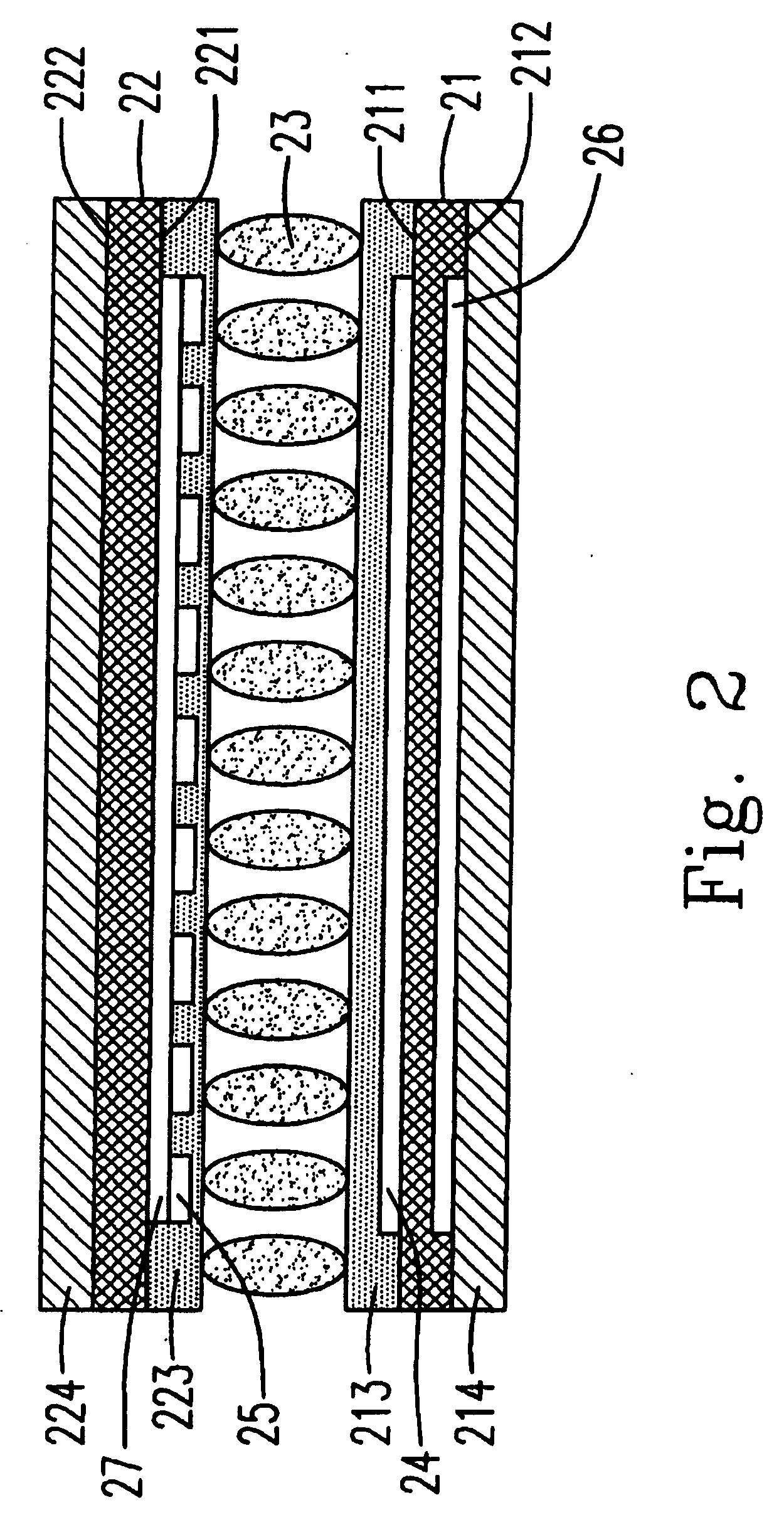
[0030] Please refer to FIG. 2, which is a diagram showing the structure of the LCD panel according to a preferred embodiment of the present invention. The liquid crystal display panel includes the first polarized substrate 21, the first alignment film 213, the first transparent electrode 24, the second polarized substrate 22, the second alignment film 223, the second transparent electrode 25 and the liquid crystal layer 23. The first polarized substrate 21 has a first surface 211 and a second surface 212 and the second polarized substrate 22 has a third surface 221 and a fourth surface 222. The first and second alignment films ...


PUM


Abstract

A liquid crystal display panel is provided. The liquid crystal display panel includes a first polarized substrate having a first surface and a second surface, a first alignment film mounted on the first surface, a first transparent electrode mounted between the first surface and the first alignment film, a second polarized substrate having a third surface and a fourth surface, a second alignment film mounted on the third surface, a second transparent electrode mounted between the third surface and the second alignment film and a liquid crystal layer, wherein the first polarized substrate and the second polarized substrate are so positioned that the first surface is near the third surface than the second surface, and the liquid crystal layer is placed therebetween.

Description

FIELD OF THE INVENTION [0001] The present invention relates to a liquid crystal display panel, and more particularly to a polarizer of a liquid crystal display panel. BACKGROUND OF THE INVENTION [0002] The active thin film transistor (TFT) is the control elements for actively controlling the light flux of each individual pixel. The principle of the image generation is that the desired color is generated by each individual pixel on the panel. To achieve this purpose, a back light is used which is normally formed by a number of fluorescent lamps. In order to light a single pixel, the panel should be divided into a number of ‘shutters’ or ‘doors’ to let the light pass through. The liquid crystal display (LCD) stands for displays that are based on liquid crystals. The molecular structures of the liquid crystal could be changed and therefore varying levels of light are able to pass through them (or the light could be blocked completely). How much light is allowed to pass and which colors...

Claims


Application Information

Patent Timeline
IPC IPC(8): G02F1/1335
CPCG02F1/133528G02F1/133305
Inventor CHEN, RUEY-SHII
Owner ARIMA DISPLAY
Why Eureka
Eureka Blog
Learn More