
Solid-state imaging device and manufacturing method of solid-state imaging device

a solid-state imaging and manufacturing method technology, applied in the field of solid-state imaging devices, can solve the problems of unable to slim down such a solid-state imaging device without sacrificing its sensitivity, and it is difficult to maintain a high light condensing efficiency to photodiodes, etc., to achieve the effect of improving picture quality, easy microlenses, and low cos

Inactive Publication Date: 2006-02-09
COLLABO INNOVATIONS INC
View PDF4 Cites 29 Cited by
  • Summary
  • Abstract
  • Description
  • Claims
  • Application Information

AI Technical Summary

Benefits of technology

[0014] Therefore, the present invention is conceived considering the problem. An object of the present invention is to provide a slim solid-state imaging device that is capable of improving picture quality without sacrificing its sensitivity and the manufacturing method of the solid-state imaging device.
[0024] Since the present invention can realize a compact camera having an excellent picture quality, and thus the present invention is highly industrially practical. FURTHER INFORMATION ABOUT TECHNICAL BACKGROUND TO THIS APPLICATION

Problems solved by technology

However, the CCD type solid-state imaging device disclosed in Japanese Laid-Open Patent Application No. 10-229180 publication has a problem that it cannot be slimed down because of the following reasons.
However, since the allowable distance ranges of displacement of such microlenses are restricted depending on the distances between adjacent microlenses, it is impossible to slim down such a solid-state imaging device without sacrificing its sensitivity.
At this time, since the size of each unit cell becomes smaller accompanied by increase in the number of pixels of the solid-state imaging device, it becomes difficult to maintain a high light condensing efficiency to photodiodes when trying to increase the number of pixels of the solid-state imaging device on the purpose of improving the picture quality.
Therefore, when trying to increase the number of pixels of the solid-state imaging device and slim down the device concurrently, this problem becomes especially troublesome.

Method used


Image

  • Solid-state imaging device and manufacturing method of solid-state imaging device
  • Solid-state imaging device and manufacturing method of solid-state imaging device
  • Solid-state imaging device and manufacturing method of solid-state imaging device

Examples


second embodiment

[0078] A camera that mounts a solid-state imaging device in this embodiment of the present invention will be described below with reference to figures.

[0079]FIG. 12 is a block diagram of a camera in the second embodiment.

[0080] As shown in FIG. 12, the camera includes: a lens 90; a solid-state imaging device 91; a driving circuit 92; a signal processing unit 93 and an external interface unit 94.

[0081] In the camera having the above-described structure, the processing until a signal is outputted to outside will be performed in the following order.

[0082] (1) Light passes through the lens 90 and enters the solid-state imaging device 91.

[0083] (2) The signal processing unit 93 drives the solid-state imaging device 91 using the driving circuit 92 and intakes the output signal from the solid-state imaging device 91.

[0084] (3) The signal processed by the signal processing unit 93 is outputted to outside through the external interface unit 94.

[0085] As described above, with the camer...


PUM


Abstract

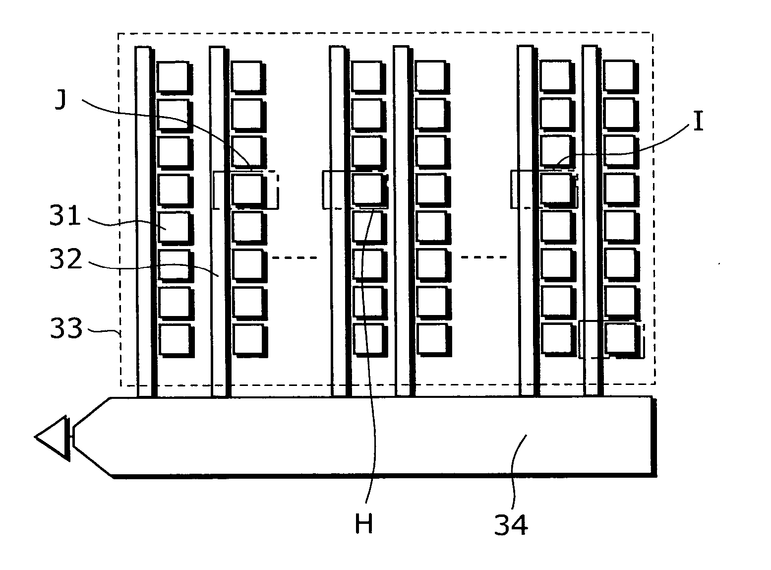
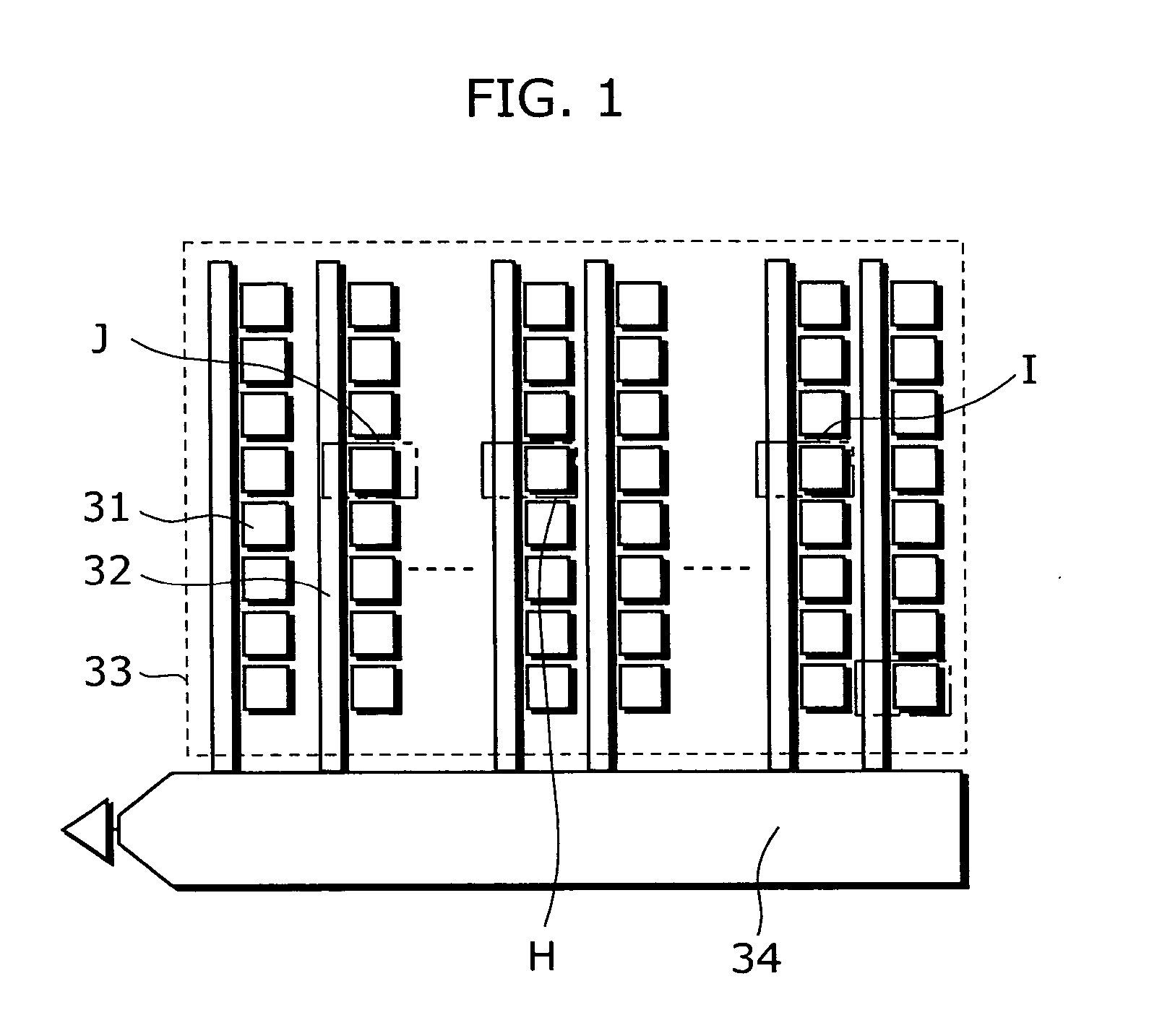
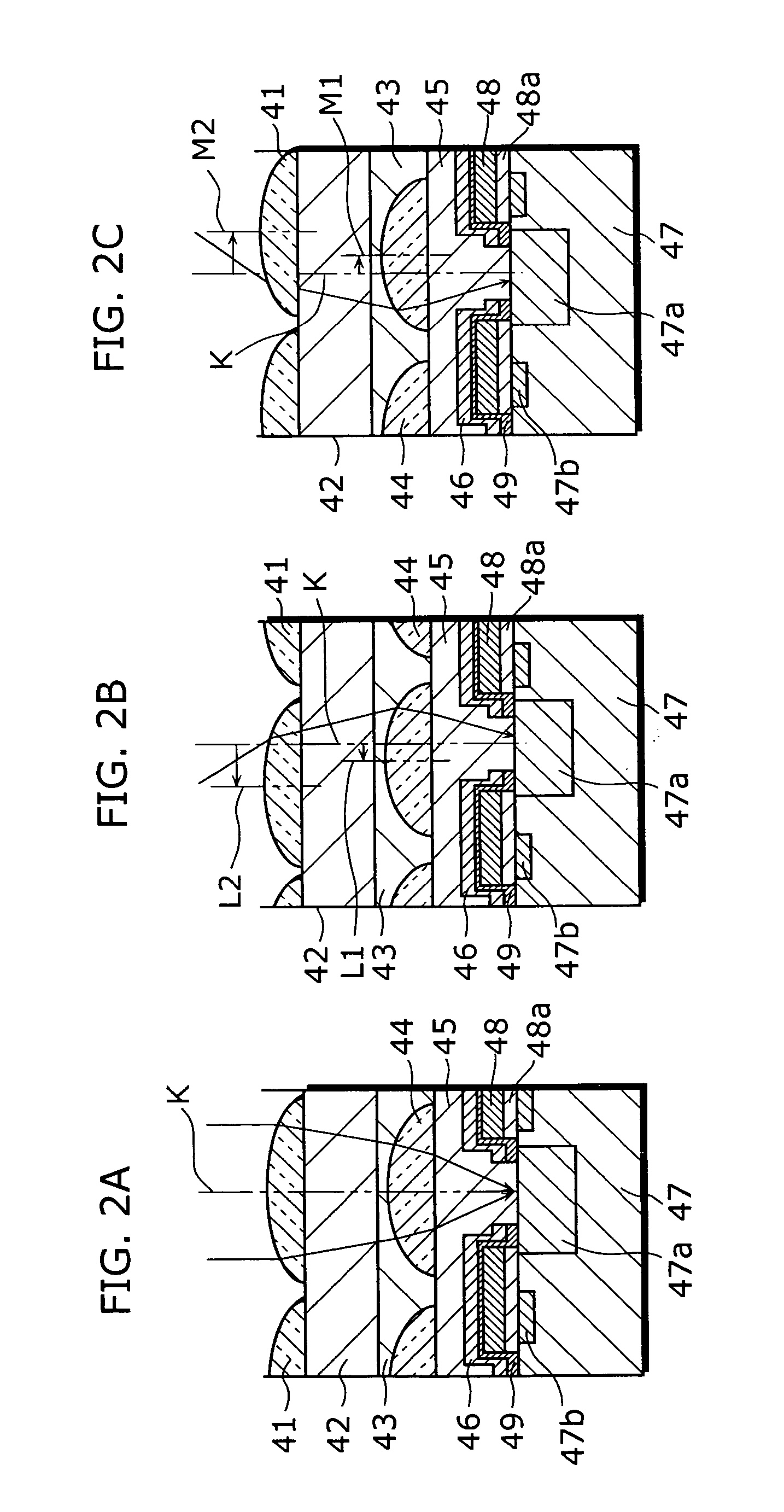
An object of the present invention is to provide a solid-state imaging device that can be slimmed down and have an improved picture quality without sacrificing its sensitivity and the manufacturing method of the solid-state imaging device. The solid-state imaging device includes an imaging unit where unit cells are arranged in a two-dimensional array. Each of these unit cells has a photodiode and a first microlens and a second microlens which are formed above the photodiode. The maximum curvatures of the convex parts become greater from the center part to the periphery of the imaging unit.

Description

BACKGROUND OF THE INVENTION [0001] (1) Field of the Invention [0002] The present invention relates to a solid-state imaging device, especially to a microlens that is placed above a photoelectric conversion element. [0003] (2) Description of the Related Art [0004] With the widespread proliferation of digital video cameras (DVDs), digital still cameras (DSCs) and mobile phones having an internal camera, the market of solid-state imaging devices has been widespread. In this movement, there is a strong demand to improve sensitivity of a solid-state imaging device. [0005] At present, a CCD type or a MOS type solid-state imaging device includes an image capturing unit where unit cells are arranged in a two-dimensional array, each of which having a photoelectric conversion element and converting a light signal obtained from a subject into an electrical signal. In a solid-state imaging device like this, its sensitivity is defined by the magnitude of output currents of photoelectric conversi...

Claims


Application Information

Patent Timeline
Patent Type & Authority Applications(United States)
IPC IPC(8): H01L33/00G02B3/00H01L27/14H04N25/00
CPCH01L27/14685H01L27/14627
Inventor KURIYAMA, TOSHIHIRO
Owner COLLABO INNOVATIONS INC
Learn More