Semiconductor device and flat panel display device having the same

a technology of semiconductor layer and display device, which is applied in the direction of semiconductor layer, semiconductor device, electrical apparatus, etc., can solve the problems of degrading electrical characteristics of patterned semiconductor layer, crosstalk can occur between neighboring tfts, etc., and achieve the effect of reducing crosstalk and being easy to mak

Active Publication Date: 2006-02-09
SAMSUNG DISPLAY CO LTD
View PDF2 Cites 18 Cited by
  • Summary
  • Abstract
  • Description
  • Claims
  • Application Information

AI Technical Summary

Benefits of technology

[0008] It is yet another object of the present invention to provide a design for TFTs that reduces crosstalk between the TFTs and does not require patterning of

Problems solved by technology

Such a design has drawbacks in that crosstalk can occur between neighboring TFTs.
However, patterning the semiconductor layer, especially an organic semiconductor layer, has

Method used


Image

  • Semiconductor device and flat panel display device having the same
  • Semiconductor device and flat panel display device having the same
  • Semiconductor device and flat panel display device having the same

Examples


Embodiment Construction

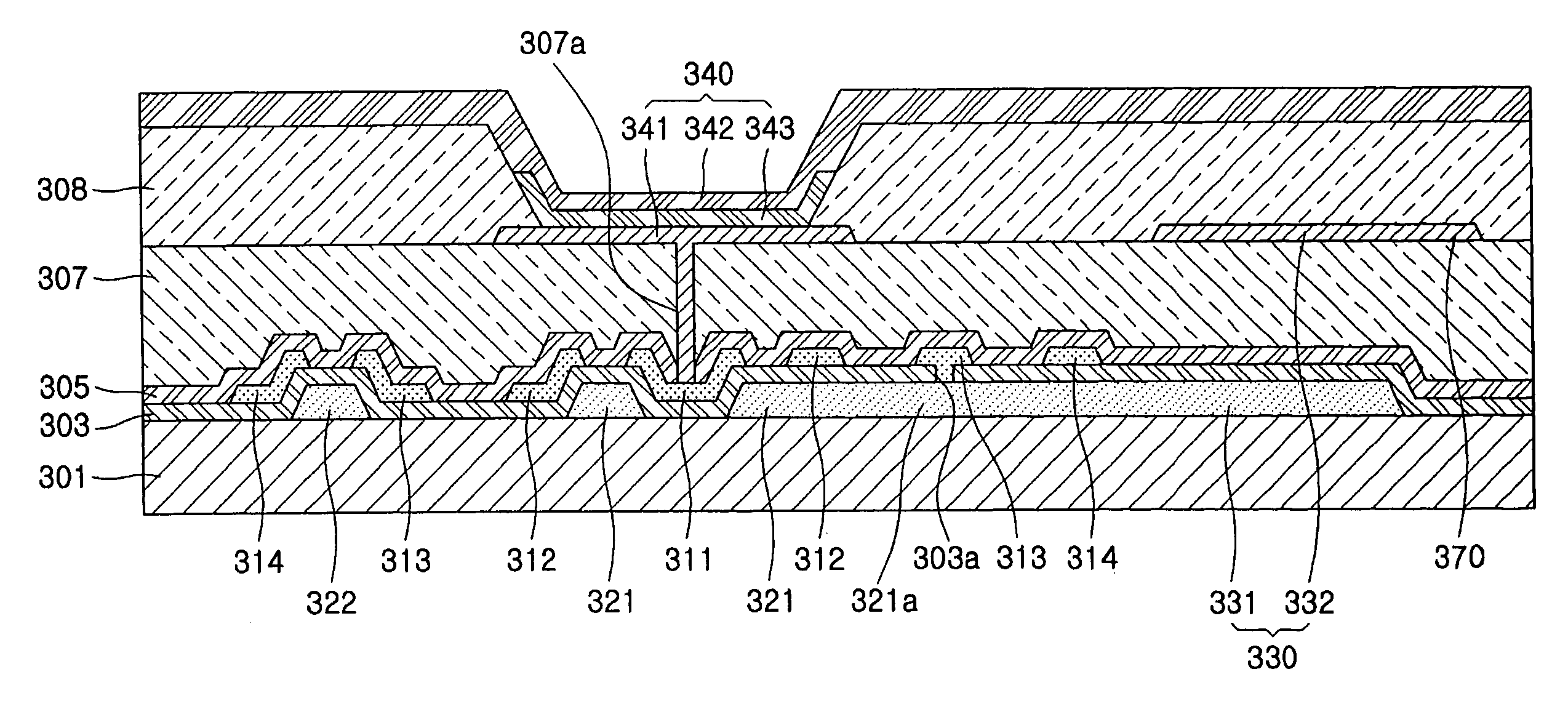
[0056] Turning now to the figures, FIG. 1 is a schematic cross-sectional view of an inverted coplanar semiconductor device having two thin film transistors (TFTs). Referring to FIG. 1, gate electrodes 21 and 22 are formed on a substrate 1, source electrodes 11 and 13 and drain electrodes 12 and 14 are formed above the gate electrodes 21 and 22, respectively, and a gate insulating layer 3 is interposed between the source electrode 11 and the gate electrode 21, between the drain electrode 12 and the gate electrode 21, between the source electrode 13 and the gate electrode 22, and between the drain electrode 14 and the gate electrode 22 so that the source electrodes 11 and 13 and the drain electrodes 12 and 14 are insulated from the gate electrodes 21 and 22. A semiconductor layer 5 contacts the source electrodes 11 and 13 and the drain electrodes 12 and 14, respectively. The source electrodes 11 and 13 and the drain electrodes 12 and 14 can be interchanged.

[0057] In the above structu...


PUM


Abstract

A semiconductor device having two thin film transistors where cross-talk is minimized and a flat panel display device having the same. The semiconductor device includes a first electrode, a second electrode surrounding the first electrode in the same plane, a third electrode surrounding the second electrode in the same plane, a fourth electrode surrounding the third electrode in the same plane, a first gate electrode insulated from the first through fourth electrodes and arranged on another plane separate from the first through fourth electrodes to correspond to a space between the first electrode and the second electrode, a second gate electrode insulated from the first through fourth electrodes and arranged on yet another plane separate from the plane of the first through fourth electrodes to correspond to a space between the third electrode and the fourth electrode, and a semiconductor layer insulated from the first gate electrode and the second gate electrode and contacting the first through fourth electrodes.

Description

CLAIM OF PRIORITY [0001] This application makes reference to, incorporates the same herein, and claims all benefits accruing under 35 U.S.C. §119 from an application for THIN FILM TRANSISTOR AND FLAT PANEL DISPLAY DEVICE THEREWITH earlier filed in the Korean Intellectual Property Office on 5 Aug. 2004 and there duly assigned Serial No. 10-2004-0061670. BACKGROUND OF THE INVENTION [0002] 1. Field of the Invention [0003] The present invention relates to a semiconductor device having thin film transistors (TFTs) and a flat panel display device having the same, and more particularly, to a semiconductor device design that minimizes cross-talk and a flat panel display device having the same. [0004] 2. Description of the Related Art [0005] Designs for coplanar TFTs often have more than on TFT formed on a substrate side-by-side with each other. On top of the electrodes of the TFTs is an unpatterned semiconductor layer. Such a design has drawbacks in that crosstalk can occur between neighbor...

Claims


Application Information

Patent Timeline
IPC IPC(8): H01L31/112
CPCH01L27/283H01L27/3262H01L27/124H01L2227/323H01L51/56H10K19/10H10K59/1213H10K59/1201H10K71/00H01L27/12H01L27/1214
Inventor KOO, JAE-BONSUH, MIN-CHUL
Owner SAMSUNG DISPLAY CO LTD
Why Eureka
Try Eureka