Image display apparatus

a technology of image display and display tube, which is applied in the direction of discharge tube/lamp details, discharge tube/lamp details, cathode ray tube/electron beam tube, etc. it can solve the problem that the getter action of the black matrix layer cannot be excellently activated, and it is difficult to obtain the large getter effect. problem, to achieve the effect of excellent activation, excellent discharging residual gas, and large getter

Inactive Publication Date: 2006-02-09
HITACHI LTD
View PDF4 Cites 7 Cited by
  • Summary
  • Abstract
  • Description
  • Claims
  • Application Information

AI Technical Summary

Benefits of technology

[0011] According to the above structure, because the conductive film that entirely covers the plural phosphors is provided with the getter action, a contact area of a material having the getter action and the FED inner space (that is, a space defined between the cathode substrate and the anode substrate) can be increased. For that reason, the large getter effect can be obtained. Also, because the conductive film is applied with a high volt...

Problems solved by technology

However, because most of the electrons from the electron emitters are inputted to the phosphors, the amount of electrons that are inputted to the black matrix layer is small.
Accordingly, in the structure...

Method used


Image

  • Image display apparatus
  • Image display apparatus
  • Image display apparatus

Examples


first embodiment

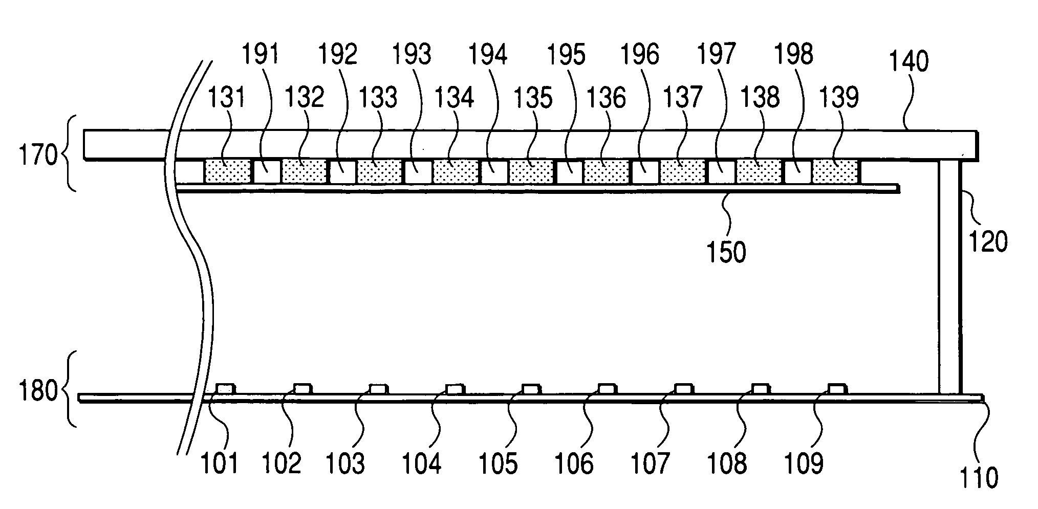
[0027] A first embodiment of the present invention will be described with reference to FIG. 1. FIG. 1 is a side view showing a section of the display panel 6 shown in FIG. 5. A cathode substrate 180 or a first substrate includes a rear glass 110, on which a plurality of electron emitters 101 to 109 are formed. In FIG. 1, the scanning lines 51 to 53 and the signal lines 41 to 44 shown in FIG. 5 are omitted from the drawing. On the other hand, an anode substrate 170 or a second substrate includes a front glass 140 having translucency, and phosphors 131 to 139 are disposed on a surface of the front glass 140 which faces the cathode substrate 180. The phosphors 131 to 139 are disposed at positions corresponding to the electron emitters 101 to 109 on the cathode substrate 180, respectively. Then, an electrically conductive film 160 or a metal back mainly made of metal is disposed on the side of the cathode substrate 180 of the phosphors 131 to 139. The conductive film 150 entirely covers...

second embodiment

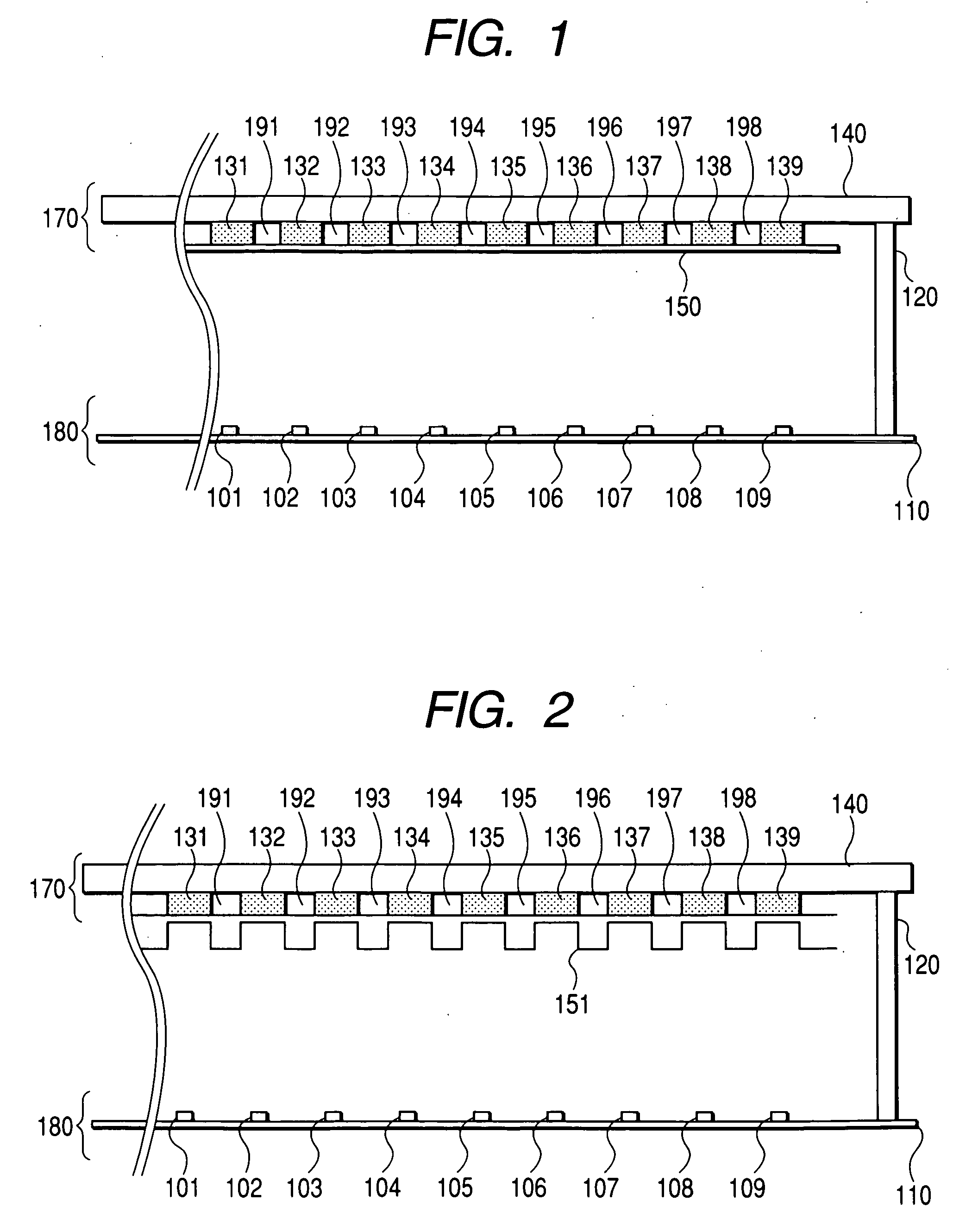
[0032] A second embodiment of the present invention will next be described with reference to FIG. 2. In FIG. 2, the same symbols as those in FIG. 1 have the identical functions. This embodiment is characterized in that in the conductive film 152 portions located at the non-emission portions between each phosphor 131 to 139, that is, at respective positions corresponding to the black matrixes 191 to 198 are formed to project toward the cathode substrate side. That is, the conductive film 151 according to this embodiment is thinner in thickness at first positions corresponding to the phosphors 131 to 139, and thicker at second positions corresponding to the black matrixes 191 to 198 than at the first positions. A material of the conductive film 151 is the same as that described in the first embodiment, and the conductive film 151 has the same getter action as that of the conductive film 150.

[0033] The electrons emitted from the electron emitters 101 to 109 lose their energy while the...


PUM


Abstract

An image display apparatus that can keep a high-vacuum level by excellently discharging a residual gas in a space within an FED. The image display apparatus has a cathode substrate on which plural electron emitters that emit electrons are disposed, and an anode substrate having translucency which is disposed opposite to the cathode substrate. The anode substrate has plural phosphors that emit light due to electrons from the electron emitters, and an electrically conductive film that is positioned on the phosphors on the side of the cathode substrate and applied with a high voltage that accelerates electrons from the electron emitters. The conductive film is provided with a getter action that adsorbs a gas within a space defined between the cathode substrate and the anode substrate.

Description

CLAIM OF PRIORITY [0001] The present application claims priority from Japanese application serial no. P2004-227418, filed on Aug. 4, 2004, the content of which is hereby incorporated by reference into this application. BACKGROUND OF THE INVENTION [0002] (1) Field of the Invention [0003] The present invention relates to image display apparatuses such as field emission displays (FED), and more particularly to an image display apparatus configured to satisfactorily increase the vacuum level therein. [0004] (2) Description of the Related Art [0005] The FED includes a cathode substrate on which a plurality of electron emitters, and an anode substrate having phosphors which is disposed opposite to the cathode substrate. Electrons from the electron emitters are allowed to collide with the phosphors, as a result of which the phosphors excitedly emit light to form an image. [0006] In the FED having the above structure, in order to make the electron emission operation of the electron emitters...

Claims


Application Information

Patent Timeline
IPC IPC(8): H01J1/62H01J63/04
CPCH01J29/085H01J31/127H01J29/94
Inventor SATOH, JUNICHIHARUNA, FUMIO
Owner HITACHI LTD
Why Eureka
Try Eureka