Light emitting device display circuit and drive method thereof

a technology of light emitting devices and display circuits, which is applied in the direction of electric digital data processing, instruments, computing, etc., can solve the problem that scanning electrodes do not supply a major part of the drive current, and achieve the effect of reducing the resistance of another main power delivering electrod

Inactive Publication Date: 2006-02-09
CHOU CHEN JEAN
View PDF13 Cites 47 Cited by
  • Summary
  • Abstract
  • Description
  • Claims
  • Application Information

AI Technical Summary

Benefits of technology

[0014] The present invention provides a method to operate a light emitting device display wherein the drive power is delivered via the same scanning electrodes that perform pixel selection for data input. A pixel circuit and drive method are provided to allow a scanning electrode (now named as scan-power electrode in this invention) performs a dual functions of selecting and controlling data input to the pixel, and delivering drive current to the light emitting element in the pixel. Furthermore, such direct current paths provided by the control circuit in a pixel in this invention is fully controlled by the signal voltages applied to said scan-power electrodes without relying on additional control signals operated on separate control lines. Alternating direct current paths are thus created via the same scan-power electrodes, and a drive current in full capacity is delivered to the light emitting elements, rather than assisting in part to reduce the resistance of another main power delivering electrode, without having to distinctively switching the power electrodes.

Problems solved by technology

Such scanning electrodes did not operate to supply a major part of the drive current to the light emitting device for producing light output, nor did such prior art pixel structures operate with any direct conducting path from a scanning electrode to the light emitting device.

Method used


Image

  • Light emitting device display circuit and drive method thereof
  • Light emitting device display circuit and drive method thereof
  • Light emitting device display circuit and drive method thereof

Examples


Embodiment Construction

[0026] Preferred embodiments of the present invention are herein described using organic light emitting diodes as illustration. Examples of using organic material to form an LED are found in U.S. Pat. No. 5,482,896 and U.S. Pat. No. 5,408,109, and examples of using organic light emitting diode to form active matrix display devices are found in U.S. Pat. No. 5,684,365 and U.S. Pat. No. 6,157,356, all of which are hereby incorporated by reference.

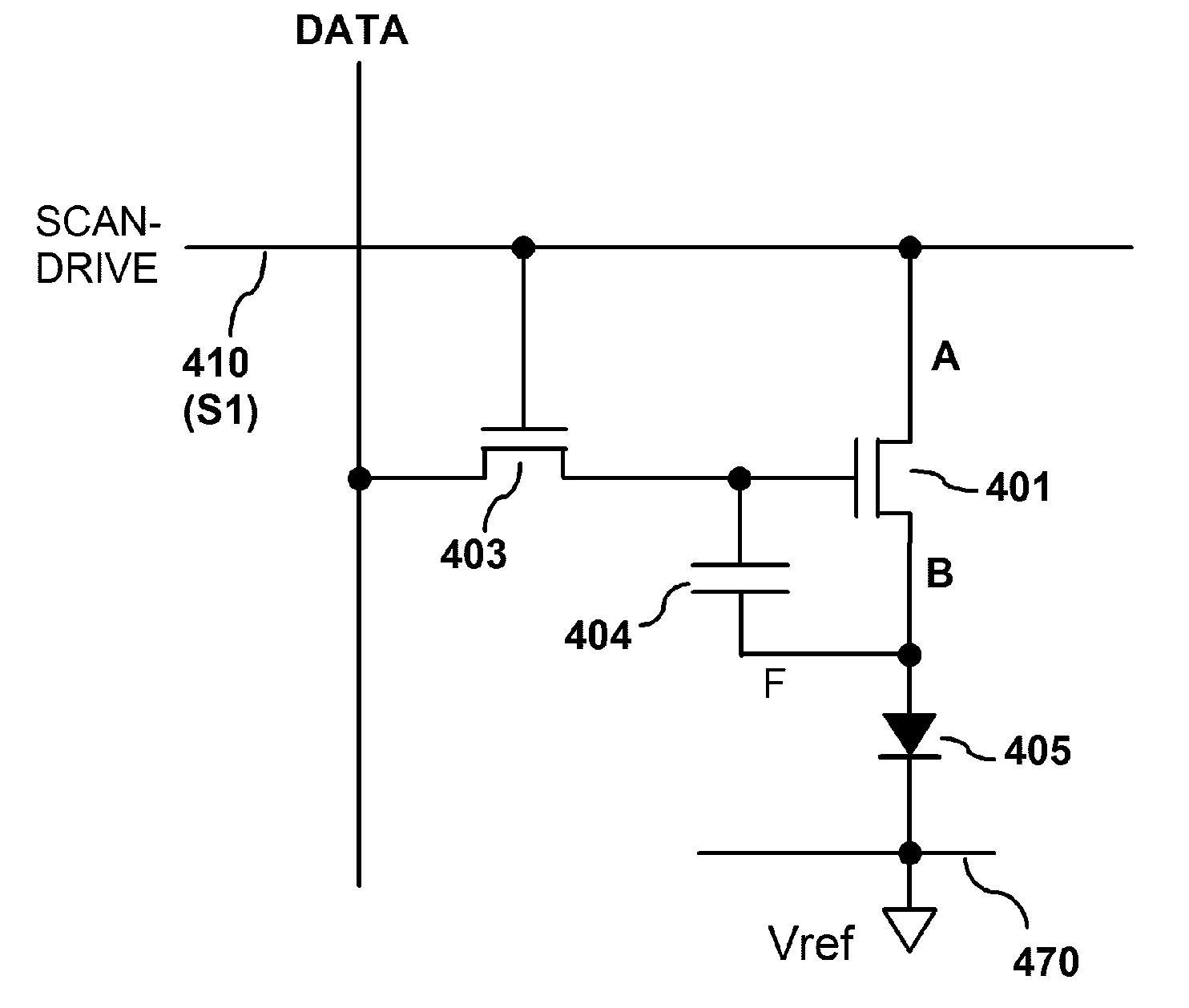
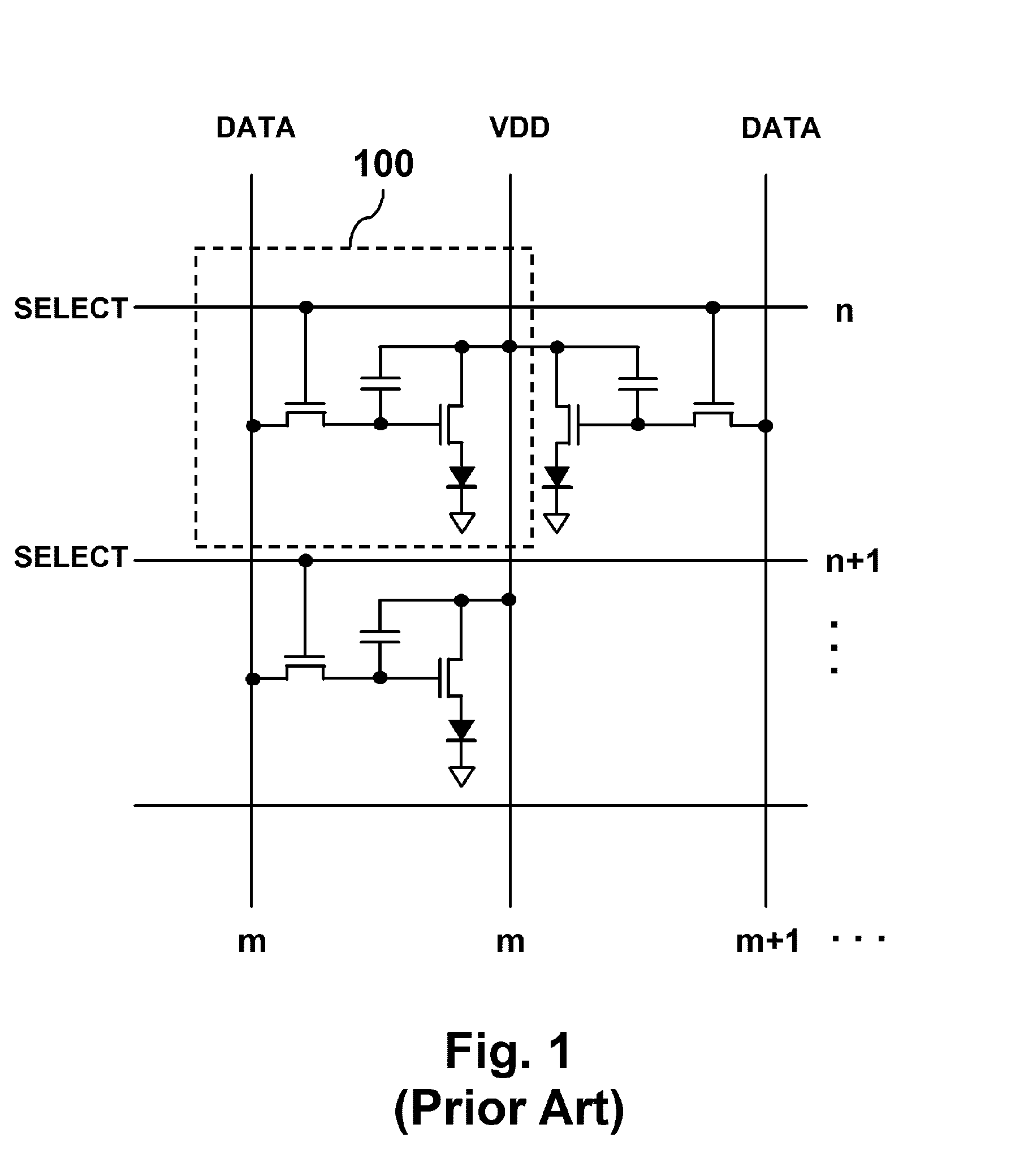
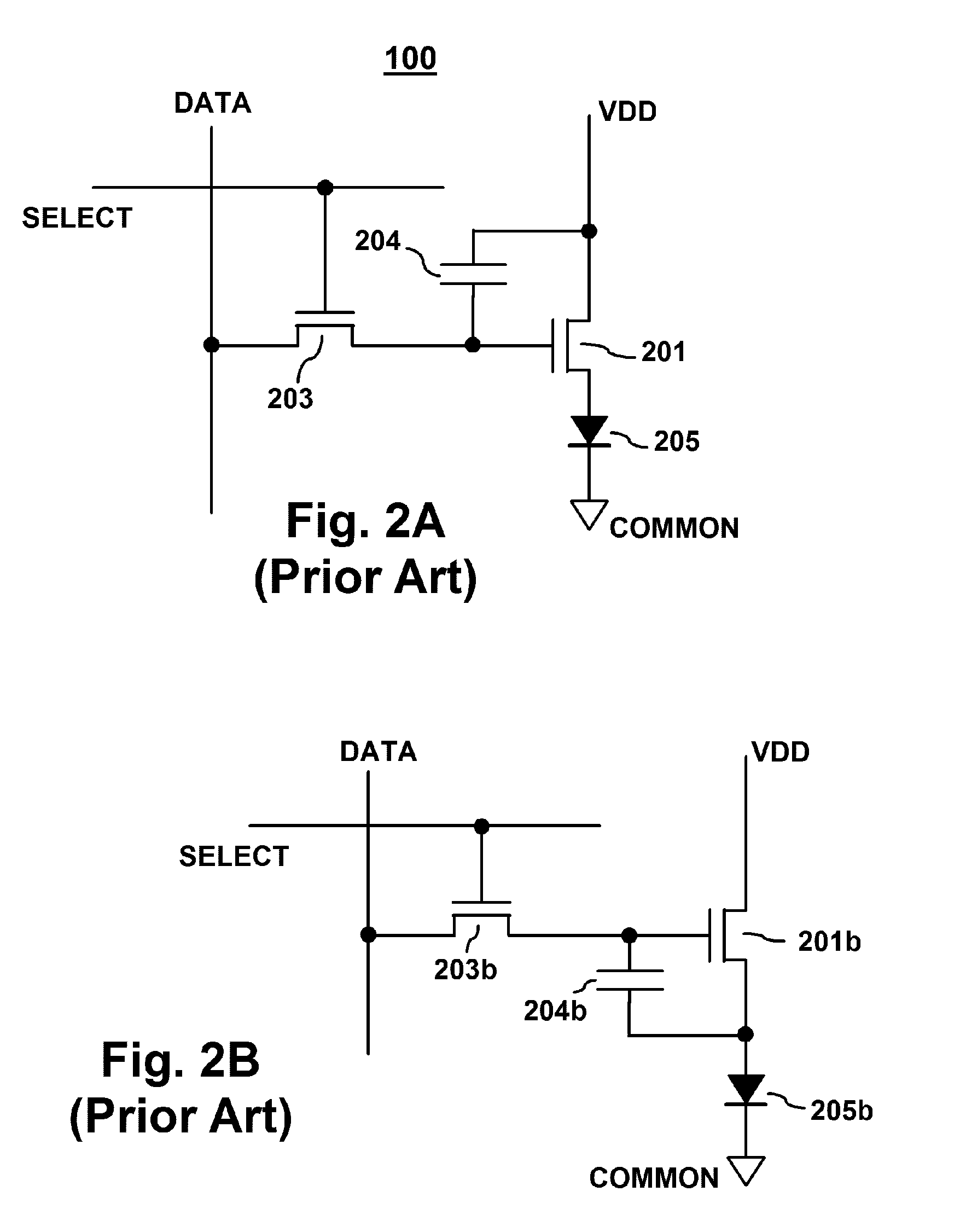
[0027] As evidenced in the prior art, the conventional method of constructing and operating a light emitting device display involves a scanning electrode (or referred to as SELECT line, GATE line, or other names carrying similar meaning) and a power supply electrode (VDD). The scanning electrode interacts with a pixel through high impedance gates of switching elements in the pixel and does not participate in delivering of drive current to the light emitting device.

[0028] The present invention provides a method to drive light emitting device...


PUM


Abstract

A driving scheme and pixel circuits therein for active matrix light-emitting device displays are provided. The driving scheme is structured to perform both line selection of and power delivery to the pixels via the same scan-power electrode, as opposed to conventional approach where scanning and drive are performed via separate access lines, thereby allowing more compact pixel design and better utilization of light emitting area. Furthermore, this driving scheme provides a dynamic reference for the active elements in a pixel, creating a different design concept and greater flexibility for pixel circuits. Embodiments of pixel circuits employing this driving scheme are exemplified in this disclosure.

Description

CROSS REFERENCE [0001] This application claims the priority of U.S. Provisional Patent Application No. 60 / 522,045, filed on Aug. 6, 2004, which is herein incorporated by reference.BACKGROUND OF THE INVENTION [0002] 1. Field of the Invention [0003] The present invention relates to the pixel circuit and a driving method of an active matrix display comprising light-emitting devices which emits light by conducting a driving current through a light emitting thin film such as an organic semiconductor thin film, and thin film transistors for controlling the light emitting operation of the respective light emitting devices. A preferred embodiment of the present invention applies to light emitting devices formed with organic material, the organic light emitting diode (OLED). More specifically, the present invention provides a method and structure to address and deliver the driving power to a pixel using multi-functional access lines, thereby simplifying the array structure of a light emittin...

Claims


Application Information

Patent Timeline
IPC IPC(8): G09G3/30
CPCG09G3/3233G09G3/3266G09G2330/02G09G2300/0842G09G2300/0465
Inventor CHOU, CHEN-JEAN
Owner CHOU CHEN JEAN
Why Eureka
Try Eureka