
Structure and method of liner air gap formation

a technology of air gap and structure, applied in the direction of solid-state device manufacturing, electric devices, semiconductor/solid-state devices, etc., to achieve the effect of reducing repetition

Active Publication Date: 2006-02-09
CHARTERED SEMICONDUCTOR MANUFACTURING
View PDF7 Cites 66 Cited by
  • Summary
  • Abstract
  • Description
  • Claims
  • Application Information

AI Technical Summary

Benefits of technology

[0019] The above and below advantages and features are of representative embodiments only, and are not exhaustive and/or exclusive. They are presented only to assist in understanding the invention. It should be understood that they are not representative of all the inventions defined by the claims, to be considered limitations on the invention as defined by the claims, or limitations on equivalents to the claims. For instance, some of these advantages may be mutually contradictory, in that they cannot be simultaneously present in a single embodiment. Similarly, some advantages

Problems solved by technology

For instance, some of these advantages may be mutually contradictory, in that they cannot be simultaneously present in a single embodiment.

Method used


Image

  • Structure and method of liner air gap formation
  • Structure and method of liner air gap formation
  • Structure and method of liner air gap formation

Examples


Embodiment Construction

I. Overview

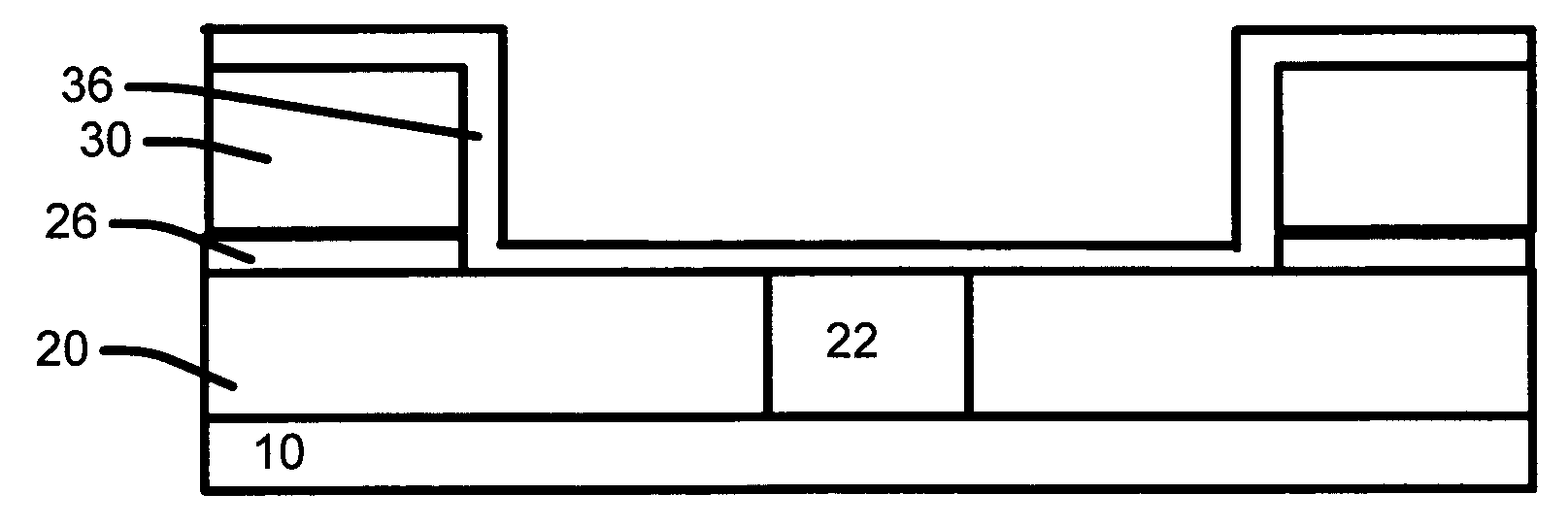
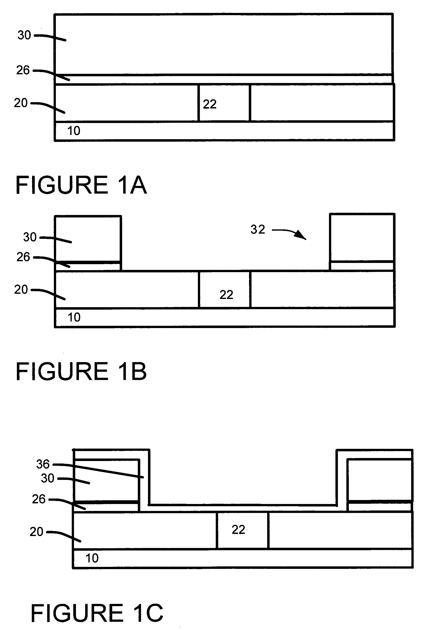
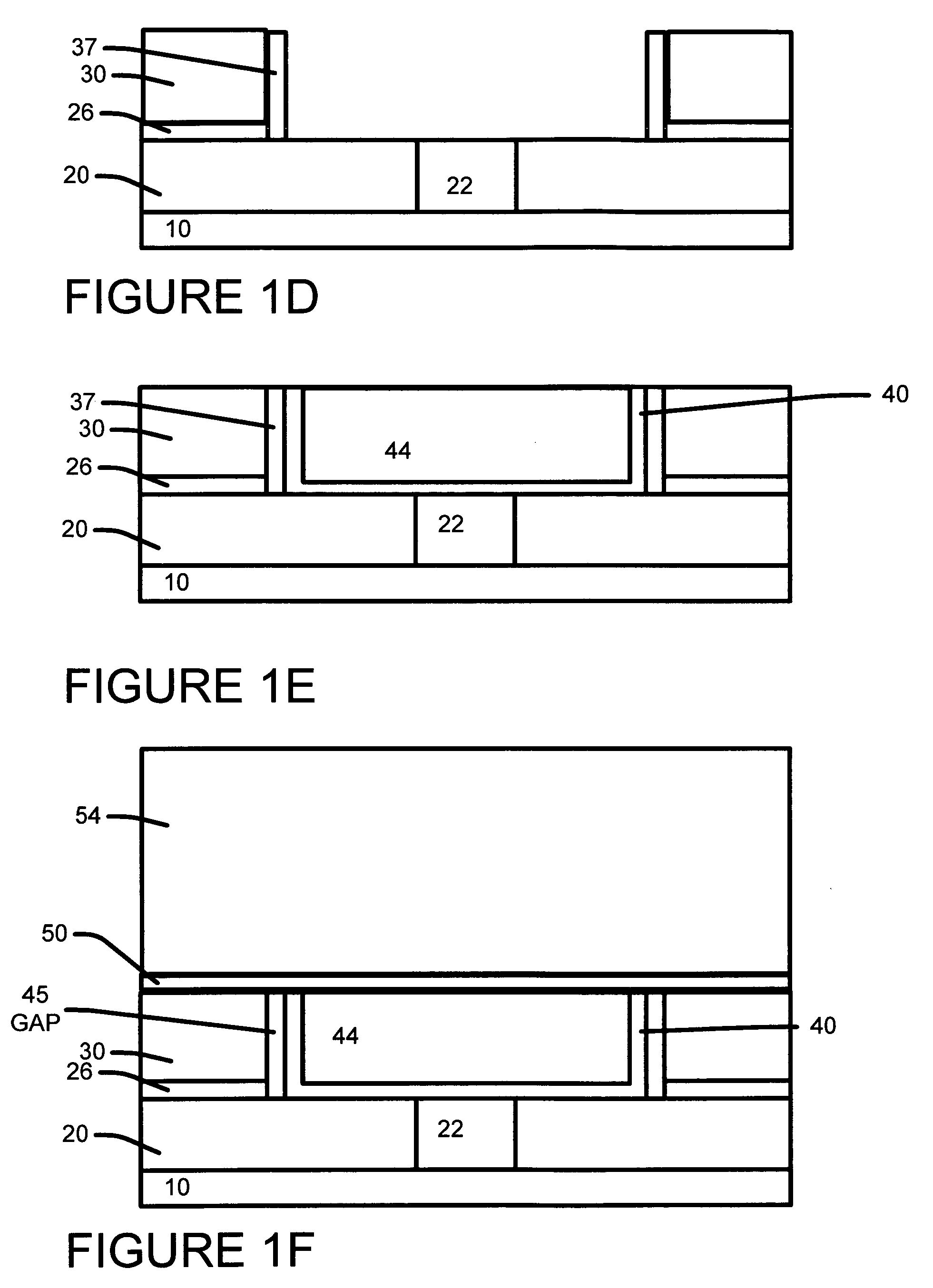
[0024] The example embodiments of the present invention will be described in detail with reference to the accompanying drawings. The example embodiments of the present invention provide structure and a method of forming a liner air gaps for interconnects.

[0025] Embodiments show an integration scheme to form liner air gaps adjacent to and / or surrounding metal lines and vias. The presence of liner air gaps can significantly reduce the effective intra-metal dielectric constant.

[0026] Note, the description and claims may describe layers and interconnects as first, second, (e.g., levels) etc., but these are relative terms and layers or interconnect can be formed at any level.

[0027] An example embodiment for fabrication of liner gap in a semiconductor device is described below. There are three preferred non-limiting options to form the sacrificial lines. (See FIGS. 1H, 1I, 1J (1st option), FIGS. 2A-2C(2nd option), FIGS. 3A-3C(3rd option).)

Form an ILD Layer

[0028] Referring...


PUM


Abstract

A structure and method of a semiconductor device with liner air gaps next to interconnects and dielectric layers. A dielectric layer is formed over a lower dielectric layer and a lower interconnect over a substrate. We form an interconnect opening in the dielectric layer. The opening has sidewalls of the dielectric layer. A sacrificial liner is formed over the sidewalls of the interconnect opening. An upper interconnect is formed that fills the opening. We remove the sacrificial liner / spacers to form (air) liner gaps.

Description

BACKGROUND OF INVENTION [0001] 1). Field of the Invention [0002] The embodiments of the invention relates generally to fabrication of semiconductor devices and relates to air-gap-containing metal / insulator interconnect structures for Very Large Scale Integrated (VLSI) and Ultra Large Scale Integrated (ULSI)semiconductor devices and packaging, and more particularly to structures, methods, and materials relating to the incorporation of voids, cavities or air gaps into multiple levels of multilayer interconnect structures for reducing wiring capacitance. [0003] 2). Description of the Prior Art [0004] Copper interconnects are formed using a dual damascene process. The incorporation of low-k insulator material may be accomplished by depositing an etch stop layer and a first layer of low-k dielectric material over a copper interconnect. This may be followed by an optional etch stop barrier insulator and then a second layer of low-k material. A via is then etched through the second layer o...

Claims


Application Information

Patent Timeline
IPC IPC(8): H01L21/78
CPCH01L21/76807H01L21/7682H01L23/53295H01L23/5222H01L23/53238H01L21/76831H01L2924/0002H01L2221/1063H01L2924/00
Inventor BU, XIAOMEISEE, ALEXLEE, TAE JONGZHANG, FANLIM, YEON KHENGHSIA, LIANG CHOO
Owner CHARTERED SEMICONDUCTOR MANUFACTURING
Features
  • Generate Ideas
  • Intellectual Property
  • Life Sciences
  • Materials
  • Tech Scout
  • Unparalleled Data Quality
  • Higher Quality Content
  • 60% Fewer Hallucinations
Learn More