Plasma display panel (PDP)

a technology of plasma and display panel, which is applied in the direction of instruments, tubes with electrostatic control, and address electrodes, etc., can solve the problems affecting the efficiency of discharge, etc., to achieve the effect of reducing the intensity of discharg

Inactive Publication Date: 2006-02-16
SAMSUNG SDI CO LTD
View PDF18 Cites 9 Cited by
  • Summary
  • Abstract
  • Description
  • Claims
  • Application Information

AI Technical Summary

Benefits of technology

[0015] An object of the present invention is to provide a PDP which is capable of alleviating the problem of the intensity of a discharge be...

Problems solved by technology

A significant amount of input power is lost through these steps.
Once a discharge has been generated, however, distribution of a voltage between the cathode and the anode has a distorted shape due to a difference in spatial charges generate...

Method used


Image

  • Plasma display panel (PDP)
  • Plasma display panel (PDP)
  • Plasma display panel (PDP)

Examples


first embodiment

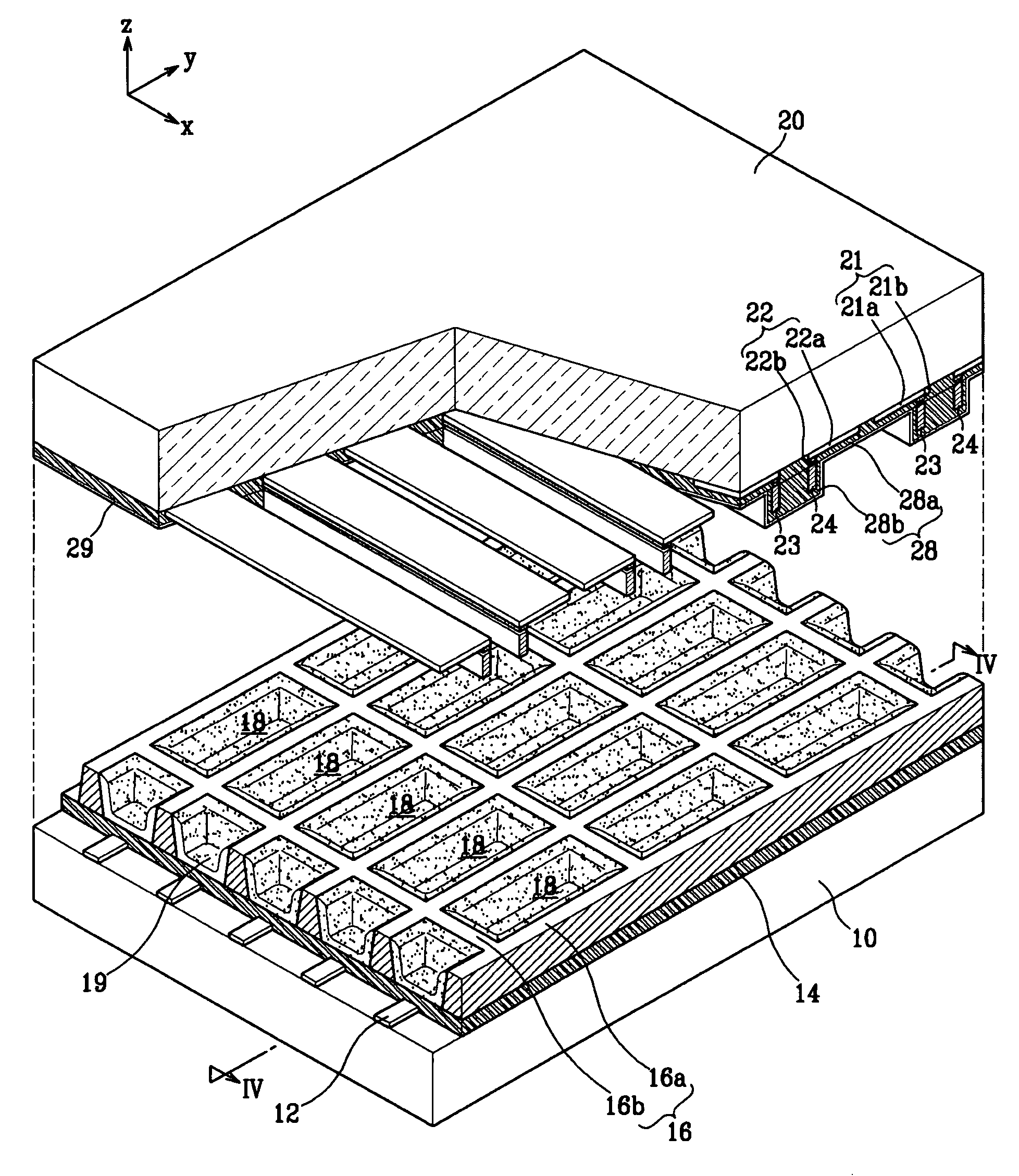
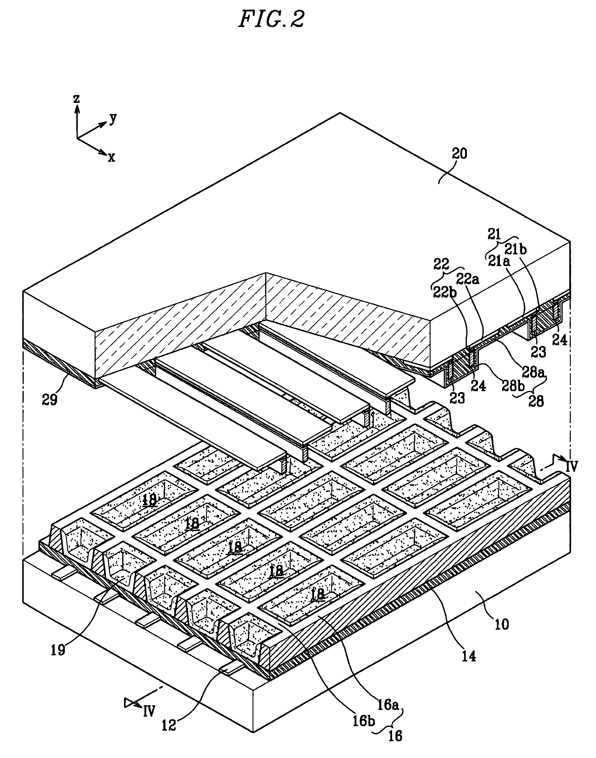
[0081]FIG. 2 is an exploded perspective view of the PDP according to the present invention. FIG. 3 is a plan view of the structure of electrodes and discharge cells in the PDP. FIG. 4 is a cross-sectional view of the PDP taken along the line IV-IV in FIG. 2.

[0082] Referring to FIGS. 2 to 4, the PDP according to the present embodiment includes a first substrate 10 (hereinafter, referred to as a “rear substrate”) and a second substrate 20 (hereinafter, referred to as a “front substrate”), which are disposed opposite to each other with a predetermined distance therebetween, and a plurality of discharge cells 18, which are defined by barrier ribs 16, in a space between the two substrates 10 and 20. Phosphor layers 19, which absorb ultraviolet light rays and emit a visible light, are formed within the discharge cells 18 along the barrier ribs and the bottom surface. The phosphor layers 19 are filled with a discharge gas (e.g., a mixed gas including Xenon (Xe), Neon (Ne) and the like) so ...

second embodiment

[0105]FIG. 8 is a plan view of the structure of electrodes and discharge cells in a PDP according to the present invention.

[0106] In the PDP according to the present embodiment, in the same manner as the first embodiment, third and third electrodes 33 and 34 are formed in the front substrate so as to be separated from the first and second electrodes 21 and 22. The third and fourth electrodes 33 and 34 are projected toward the rear substrate in a direction away from the front substrate. The third and fourth electrodes 33 and 34 are formed to face each other with a space therebetween. The space can induce an opposite discharge between the third and fourth electrodes 33 and 34 opposing each other. These third and fourth electrodes 33 and 34 are preferably made of a metal.

[0107] Referring to FIG. 8, in the PDP according to the present embodiment, each of the third and fourth electrodes 33 and 34 includes a plurality of unit electrodes, which are separated from each other and arranged p...

third embodiment

[0108]FIGS. 9A to 9D are cross-sectional views of a PDP according to the present invention, and show the size and location of a cathode spot and an anode spot depending upon a time after a discharge has occurred. Different signal voltage generators supply different voltages V1 to V4 to respective electrodes.

[0109] In the present embodiment, a third electrode 23 has a voltage higher than that of a first electrode 21, and a fourth electrode 24 has a voltage higher than that of a second electrode 22.

[0110] The first and third electrodes 21 and 23 are connected to different signal voltage generators (not shown), respectively, and can receive the signal voltages V1 and V3, respectively. The voltage V3 supplied to the third electrode 23 is higher than the voltage V1 supplied to the first electrode 21.

[0111] Furthermore, the second and fourth electrodes 22 and 24 are respectively connected to different signal voltage generators (not shown), and can receive the signal voltages V2 and V4. ...


PUM


Abstract

A Plasma Display Panel (PDP) includes: first and second substrates arranged opposite to each other; address electrodes arranged parallel to each other on the first substrate; barrier ribs arranged in a space between the first and second substrates to divide a plurality of discharge cells; phosphor layers respectively arranged within the discharge cells; first and second electrodes arranged on the second substrate corresponding to the respective discharge cells, the first and second electrodes extending in a direction crossing the address electrodes; and third and fourth electrodes, separated from the first and second electrodes, and projecting toward the first substrate in a direction away from the second substrate, the third and fourth electrodes facing each other with a space therebetween.

Description

CLAIM OF PRIORITY [0001] This application makes reference to, incorporates the same herein, and claims all benefits accruing under 35 U.S.C. §119 from the six (6) applications all of which are entitled PLASMA DISPLAY PANEL, and are earlier filed in the Korean Intellectual Property Office on 30 Jun. 2004, and there duly assigned Serial Nos. 10-2004-0050584, 10-2004-0050725, 10-2004-0050726, 10-2004-0050741, 10-2004-0050742 and 10-2004-0050743, respectively. BACKGROUND OF THE INVENTION [0002] 1. Field Of the Invention [0003] The present invention relates to a Plasma Display Panel (PDP) and, more particularly, to a PDP having an electrode structure which is advantageous in realizing higher density and high luminance display. [0004] 2. Description of the Related Art [0005] A Plasma Display Panel (PDP) is a display element which realizes an image using visible light generated by exciting phosphors with Vacuum UltraViolet (VUV) light radiated by a plasma obtained by the discharge of gas. ...

Claims


Application Information

Patent Timeline
IPC IPC(8): G09G3/10H01J29/00H01J11/12H01J11/14H01J11/16H01J11/22H01J11/24H01J11/26H01J11/30H01J11/32H01J11/34H01J11/36H01J11/38H01J11/40H01J11/42H01J11/44H01J11/46H01J11/50
CPCH01J11/30H01J11/12
Inventor HUR, MINCHOI, HOON-YOUNGCHOI, YOUNG-DOMIZUTA, TAKAHISACHO, YOON-HYOUNG
Owner SAMSUNG SDI CO LTD
Why Eureka
Try Eureka