Integrated circuit with increased heat transfer

a technology of integrated circuits and heat transfer, which is applied in the direction of semiconductor devices, semiconductor/solid-state device details, electrical apparatus, etc., can solve the problems of reducing the reliability and efficiency of integrated circuits, silver or gold alloys with low thermal resistance, and the lid thickness may be reduced, so as to reduce the thermal resistivity of integrated circuit dies and increase the surface area of lateral sides. , the effect of increasing the surface area

Active Publication Date: 2006-02-23
GLOBALFOUNDRIES US INC
View PDF22 Cites 11 Cited by
  • Summary
  • Abstract
  • Description
  • Claims
  • Application Information

AI Technical Summary

Benefits of technology

[0008] A technique for improving the thermal power dissipation of an integrated circuit includes reducing the thermal resistivity of the integrated circuit by increasing heat transfer in vertical and / or lateral directions. These results are achieved by increasing the surface area of the backside and / or the surface area of the lateral sides of the integrated circuit die. In some embodiments of the invention, an integrated circuit includes circuit elements formed closer to a first surface of a semiconductor substrate than to a second surface of the semiconductor substrate. The semiconductor substrate has a varying profile that substantially increases the surface area of a thermal interface formed on the second surface as compared to the second surface being substantially planar. A maximum depth of the profile is less than the thickness of the semiconductor substrate.
[0010] In some embodiments of the present invention, a method includes reducing a thermal resistivity of an integrated circuit die by increasing a surface area of a first surface of a semiconductor substrate. Circuit elements are formed closer to a second surface of the semiconductor substrate than to the first surface. A maximum depth of a profile of the first surface is less than a thickness of the semiconductor substrate.
[0011] In some embodiments of the present invention, a method includes reducing a thermal resistivity of an integrated circuit die by increasing the surface area of a first surface of a semiconductor substrate. Circuit elements are formed closer to a second surface of the semiconductor substrate than to the first surface. The method also includes reducing the thermal resistivity of the die by thermal dissipation via a thermally conductive layer formed on the first side of the die. The thermally conductive layer is electrically isolated from the circuit elements and interfaces a dielectric layer formed between the second surface of the semiconductor substrate and the circuit elements.
[0014] In some embodiments of the present invention, an integrated circuit die includes at least one lateral side of the die having a varying profile. The varying profile substantially increases the surface area of a thermal interface formed on the lateral side as compared to the lateral side being substantially planar. In some embodiments of the present invention, a method includes reducing a thermal resistivity of an integrated circuit die by increasing a surface area of a lateral side of the die. The method may include reducing the thermal resistivity of the die by thermal dissipation via a thermally conductive layer formed on the lateral side of the die.

Problems solved by technology

High temperatures of integrated circuits may decrease reliability and efficiency of the integrated circuit.
However, silver or gold alloys which have a low thermal resistance, may be cost prohibitive for the lid of typical integrated circuits.
The thickness of the lid may be reduced to reduce the lid's thermal resistance, but elimination of the lid leaves the integrated circuit vulnerable to cracking.

Method used


Image

  • Integrated circuit with increased heat transfer
  • Integrated circuit with increased heat transfer
  • Integrated circuit with increased heat transfer

Examples


Embodiment Construction

)

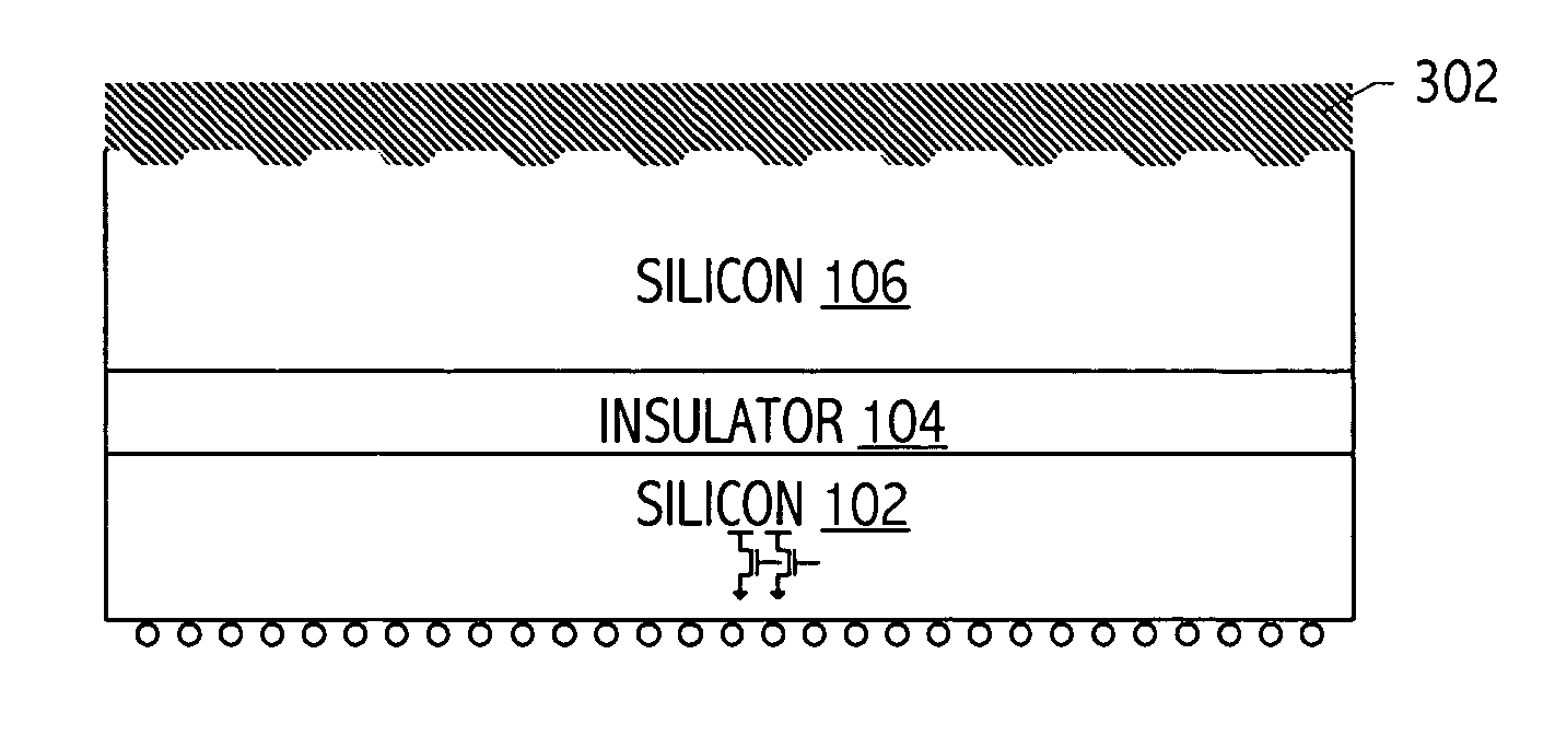
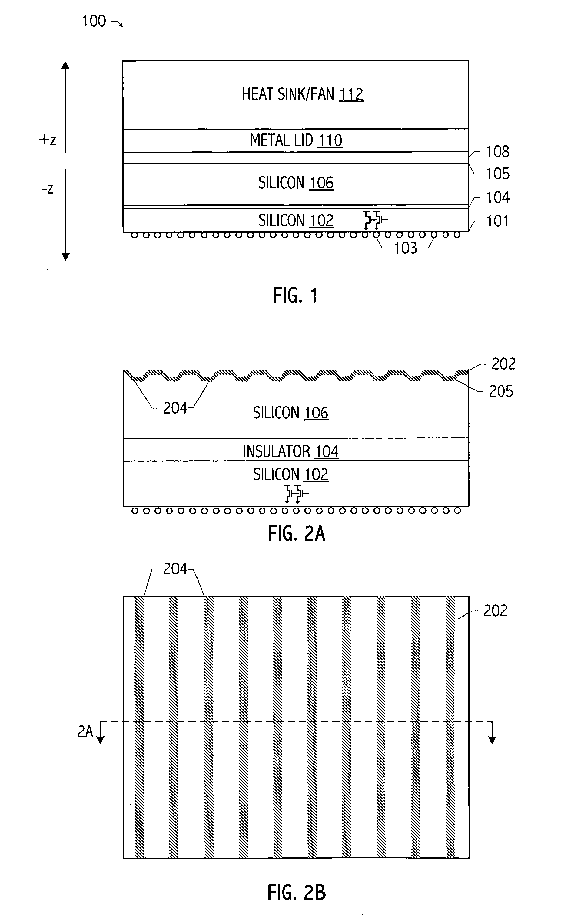
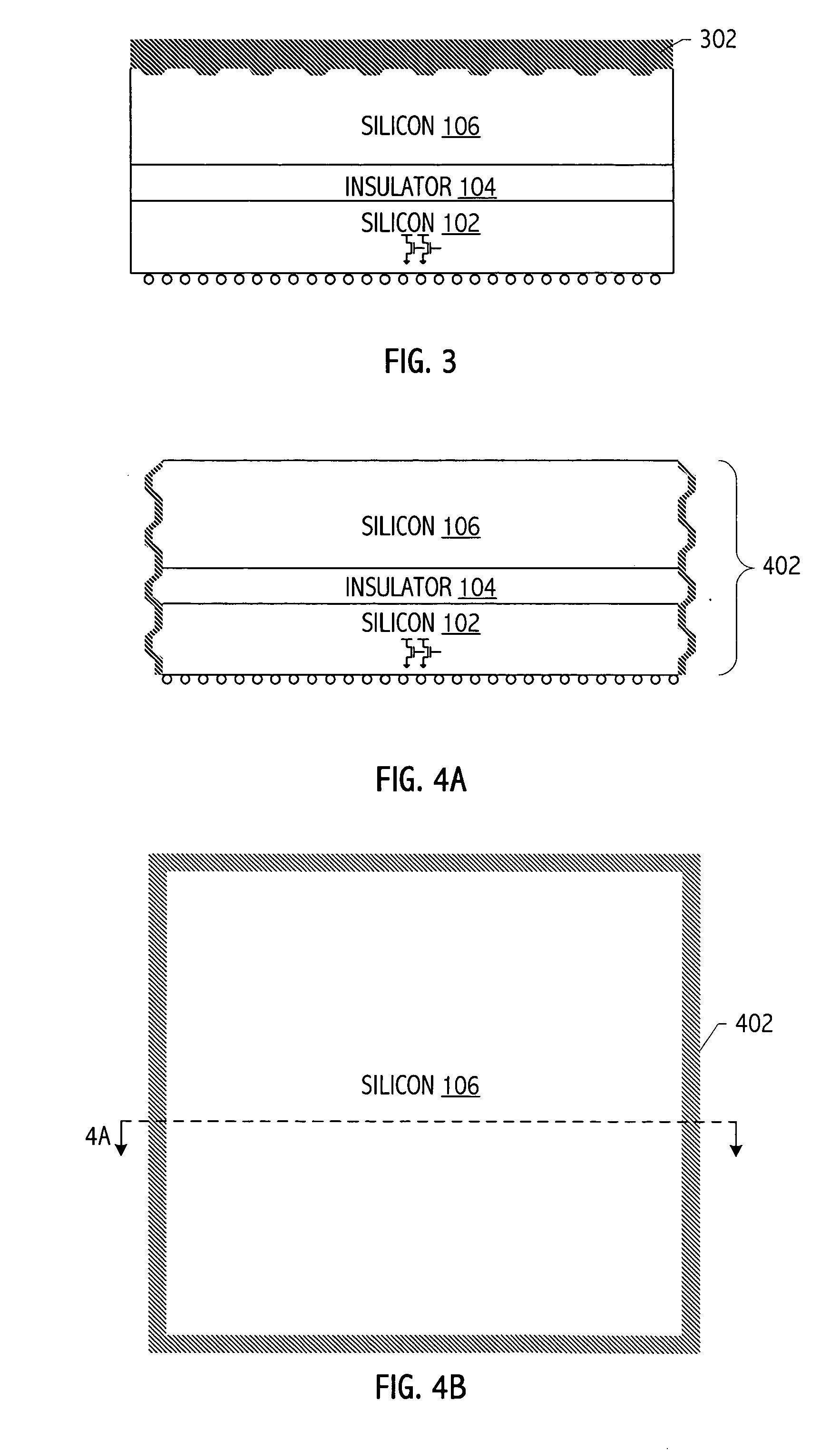
[0025] Referring to FIG. 1, an exemplary integrated circuit and cooling technique includes a silicon substrate 106, insulator layer 104, and silicon layer 102. Silicon layer 102 includes substantially all of the circuit devices in packaged integrated circuit 100. The interface, e.g., interface 101, between silicon layer 102 and conductive bumps 103 is the front side of the integrated circuit. Interface 105, i.e., the interface between silicon substrate 106 and thermal interface material (TIM) 108, is the backside of the integrated circuit and is substantially planar.

[0026] Thermal interface material 108 is included between metal lid 110 and silicon substrate 106 to eliminate air gaps produced by surface irregularities of metal lid 110 and silicon substrate 106 and to increase joint conductivity to improve heat transfer between metal lid 110 and silicon substrate 106. Thermal interface material 108 may be a thermal grease, thermally conductive compound (e.g., an aluminum compound),...


PUM


Abstract

A technique for improving the thermal power dissipation of an integrated circuit includes reducing the thermal resistivity of the integrated circuit by increasing heat transfer in vertical and / or lateral directions. These results are achieved by increasing the surface area of the backside and / or the surface area of the lateral sides of the integrated circuit die. In some embodiments of the invention, an integrated circuit includes circuit elements formed closer to a first surface of a semiconductor substrate than to a second surface of the semiconductor substrate. The semiconductor substrate has a varying profile that substantially increases the surface area of a thermal interface formed on the second surface as compared to the second surface being substantially planar. A maximum depth of the profile is less than the thickness of the semiconductor substrate.

Description

CROSS-REFERENCE TO RELATED APPLICATION(S) [0001] This application is a continuation-in-part of co-pending application Ser. No. 10 / 920,764, filed Aug. 18, 2004, entitled “INTEGRATED CIRCUIT WITH INCREASED HEAT TRANSFER” by Michael Zhuoying Su, which application is hereby incorporated by reference.BACKGROUND [0002] 1. Field of the Invention [0003] The present invention relates to integrated circuits, and more particularly to thermal power dissipation of integrated circuits. [0004] 2. Description of the Related Art [0005] High temperatures of integrated circuits may decrease reliability and efficiency of the integrated circuit. As the density of transistors on an integrated circuit increases and transistor sizes decrease, thermal power generated by the circuit increases, thus increasing the need for removing heat from a packaged integrated circuit. For example, an increase in transistor density may result in an increase in power density by a factor of two or three. [0006] The thermal r...

Claims


Application Information

Patent Timeline
Patent Type & Authority Applications(United States)
IPC IPC(8): H01L23/34
CPCH01L23/367H01L29/0657H01L2924/10158H01L2924/01079H01L2224/16H01L2924/00011H01L2924/00014H01L2224/0401
Inventor SU, MICHAEL ZHUOYINGEPPES, DAVID HARRY
Owner GLOBALFOUNDRIES US INC
Why Eureka
Try Eureka