

Self-aligned image sensor and method for fabricating the same
- Summary
- Abstract
- Description
- Claims
- Application Information
AI Technical Summary
Benefits of technology
Problems solved by technology
Method used
Image

Examples
Embodiment Construction
[0026] Reference will now be made in detail to the preferred embodiments of the present invention, examples of which are illustrated in the accompanying drawings. Wherever possible, the same reference numbers will be used throughout the drawings to refer to the same or like parts.
[0027] Hereinafter, a self-aligned image sensor and a method for fabricating the same according to the present invention will be described with reference to the accompanying drawings.
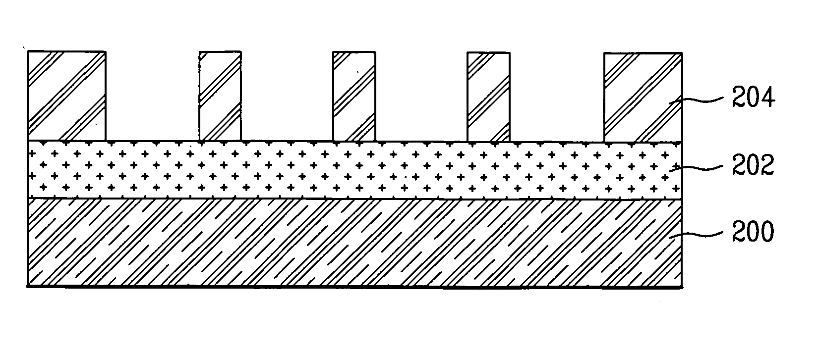
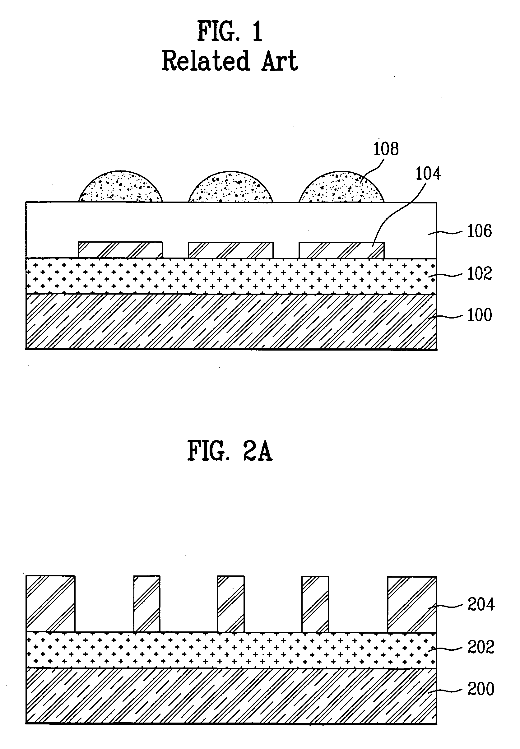
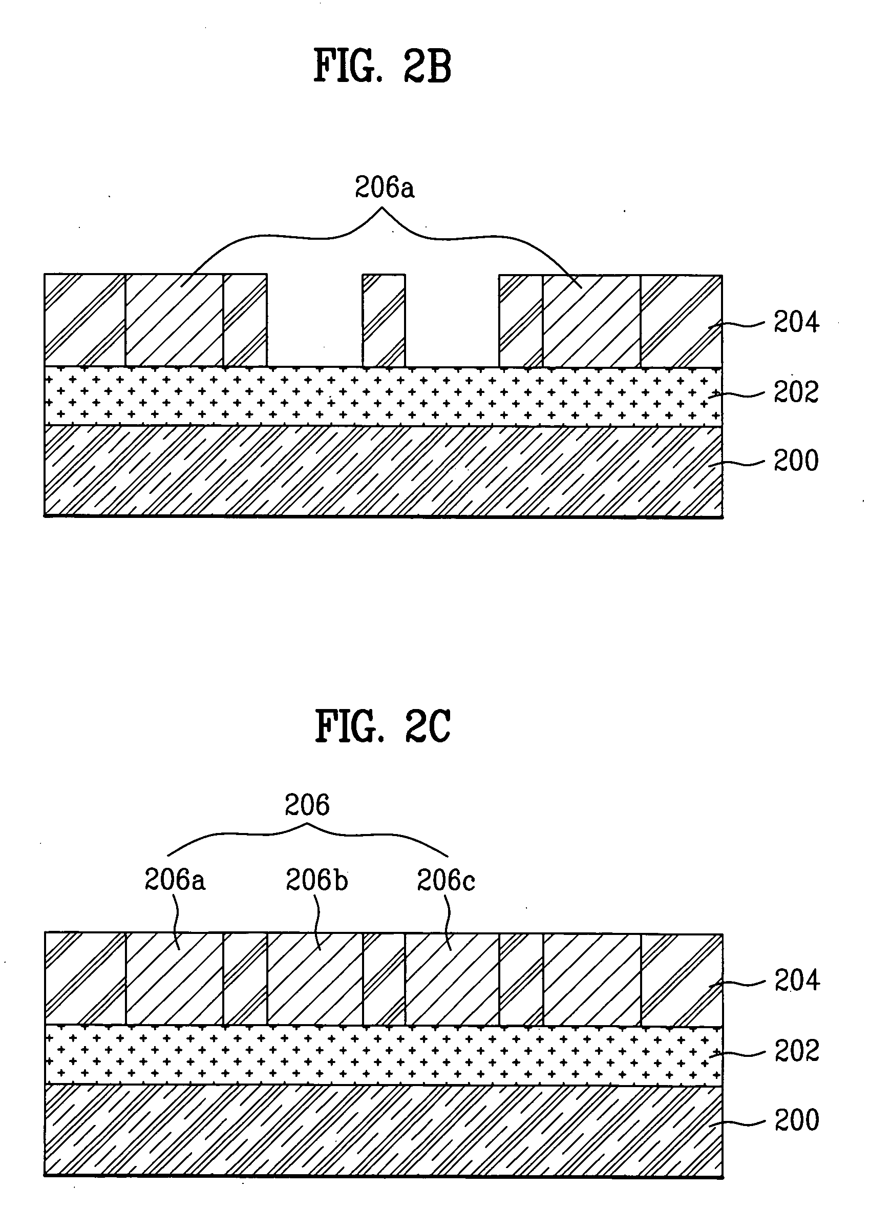
[0028]FIG. 2A to FIG. 2E are cross sectional views of the process for fabricating an image sensor according to the present invention.
[0029] First, image sensor elements (not shown) including a pixel having a light-receiving area such as a photodiode, an insulating interlayer and a metal line are formed in a semiconductor substrate 200 by an image sensor fabrication technology.
[0030] Next, as shown in FIG. 2A, a protection layer 202 is formed on the semiconductor substrate 200 (generally by chemical vapor deposition, or CVD)...
PUM
 Abstract
Description
Claims
Application Information