Patterning SOI with silicon mask to create box at different depths

a technology of soi and silicon mask, applied in the direction of semiconductor/solid-state device manufacturing, basic electric elements, electric instruments, etc., can solve the problems of different wafer levels or heights of soi devices, high defect rate in the transition region, and defect at all of the patterned edge regions

Inactive Publication Date: 2006-02-23
IBM CORP
View PDF12 Cites 33 Cited by
  • Summary
  • Abstract
  • Description
  • Claims
  • Application Information

AI Technical Summary

Benefits of technology

[0018] Applications for patterned SOI substrates have been discussed in the past, but these take advantage of a mask layer to prevent the implanted oxygen used in a SIMOX process from entering the substrate. Therefore, the masked areas never see the implanted species. In the invention described below, a mask (resist or resist/hardmask bilayer...

Problems solved by technology

Unfortunately, masked or patterned ion implantation produces a region of partial implantation, referred to as the transition region, in the semiconductor substrate.
As a result of this partial dose, the transition region is highly defective, containing crystal defects that may propagate to other regions of the semiconductor silicon layer.
This method is known to cause defects at all of the patterned edge regions.
One problem with this method is that the structure is non-planar and, therefore, the levels or heights ...

Method used


Image

  • Patterning SOI with silicon mask to create box at different depths
  • Patterning SOI with silicon mask to create box at different depths
  • Patterning SOI with silicon mask to create box at different depths

Examples


Embodiment Construction

[0031] The present invention, which provides a method of fabricating a patterned SOI substrate, will now be described in greater detail by referring to the drawings that accompany the present application. It is noted that the drawings of the present application are provided for illustrative purposes and thus they are not drawn to scale. The patterned SOI substrate formed in the present invention may comprise a substrate containing both SOI and non-SOI regions or a dual depth SOI substrate.

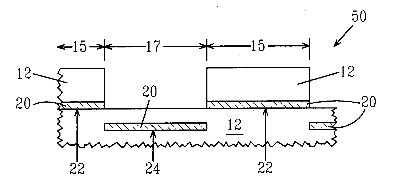
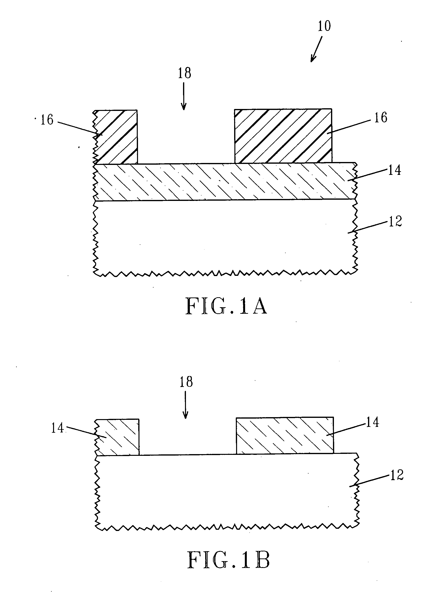
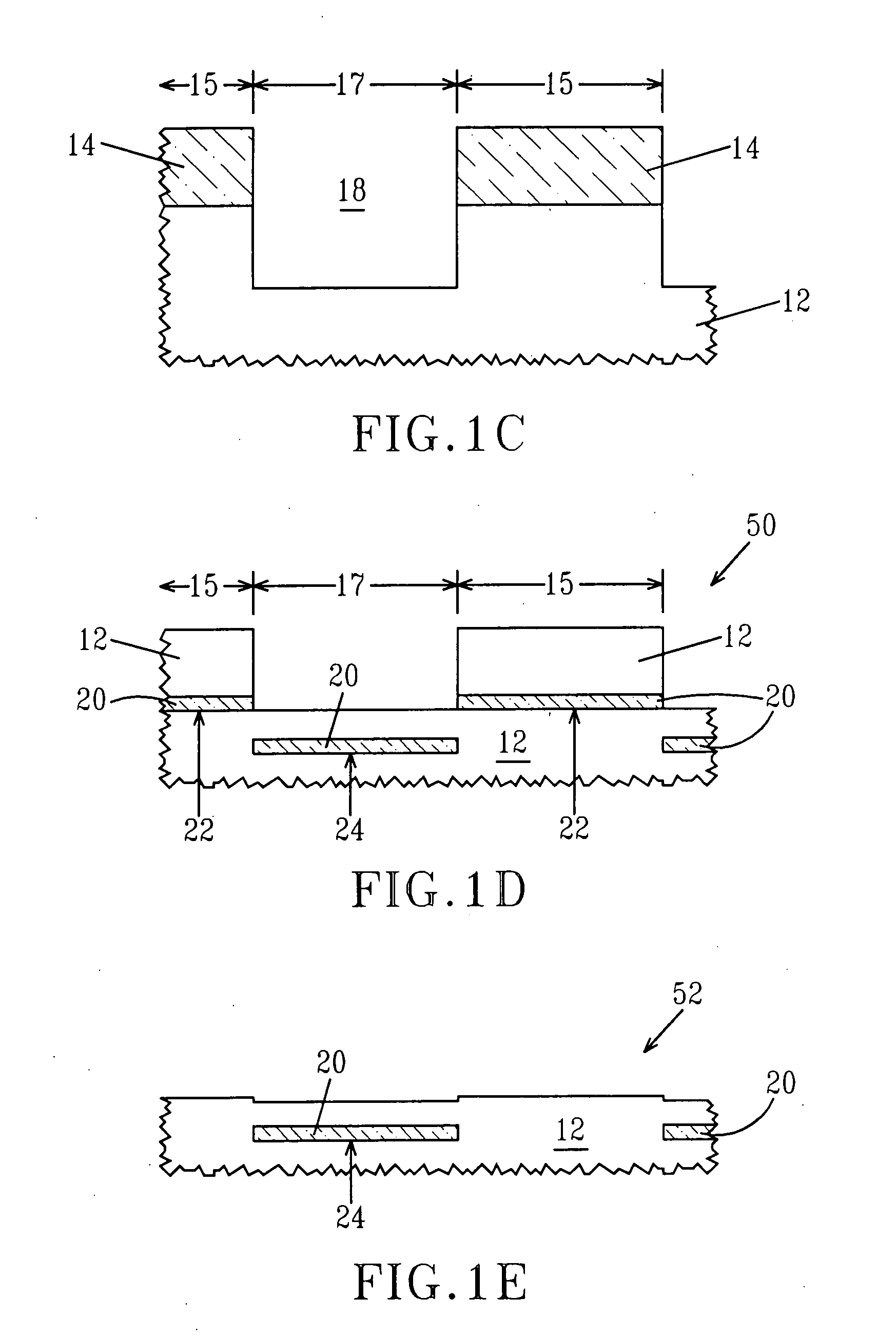
[0032] Reference is first made to FIGS. 1A-1E that illustrate one embodiment of the present invention. Specifically, the drawings depicted in FIGS. 1A-1E illustrate the processing flow used in the present invention for fabricating a patterned SOI substrate, i.e., dual depth SOI or a substrate containing SOI and non-SOI regions. The processing flow begins by providing the initial structure 10 shown in FIG. 1A. The initial structure 10 comprises a Si-containing substrate 12, an optional hardmask 14,...


PUM


Abstract

The present invention provides a method of fabricating a patterned silicon-on-insulator substrate which includes dual depth SOI regions or both SOI and non-SOI regions within the same substrate. The method of the present invention includes forming a silicon mask having at least one opening on a surface of Si-containing material, recessing the Si-containing material through the at least one opening using an etching process to provide a structure having at least one recess region and a non-recessed region, and forming a first buried insulating region in the non-recessed region and a second buried insulating region in the recessed region. In accordance with the present invention, the first buried insulating region in the non-recessed region is located above the second buried isolation region in the recessed region. A lift-off step can be employed to remove the first buried insulating region and the material that lies above to provide a substrate containing both SOI and non-SOI regions.

Description

FIELD OF THE INVENTION [0001] The present invention relates to a patterned semiconductor substrate, and more particularly to a method of fabricating a patterned semiconductor substrate that includes silicon-on-insulator (SOI) regions and non-SOI, i.e., bulk, regions within the same substrate. The method of the present invention can also provide a dual depth SOI substrate. BACKGROUND OF THE INVENTION [0002] As semiconductor technologies become more complex, there is a demand for providing semiconductor structures that have more functionality associated therewith. For example, in order to provide customers with the optimum designs, it may be required to build high performance complementary metal oxide semiconductor (CMOS) devices as well as to add additional functions such as dynamic random access memory (DRAM) or radio frequency (RF) applications. All of the devices are optimized under different conditions. For example, RF and DRAM applications have traditionally been built on bulk s...

Claims


Application Information

Patent Timeline
IPC IPC(8): H01L21/302
CPCH01L21/76224
Inventor SADANA, DEVENDRA K.SCHEPIS, DOMINIC J.STEIGERWALT, MICHAEL D.
Owner IBM CORP
Why Eureka
Try Eureka