
High power light emitting diode package

a technology of light-emitting diodes and packages, applied in the field of high-power light-emitting diodes, can solve the problems of obstructing the miniaturization of an illumination system, causing a considerable amount of heat, and burdening the manufacture cost, so as to improve the thermal radiation efficiency, simplify the construction thereof, and reduce the size and thickness

Inactive Publication Date: 2006-03-02
SAMSUNG ELECTRONICS CO LTD
View PDF2 Cites 187 Cited by
  • Summary
  • Abstract
  • Description
  • Claims
  • Application Information

AI Technical Summary

Benefits of technology

The present invention provides a high power LED package with improved thermal radiation efficiency and reduced size and thickness. The package includes a metal plate of a heat sink, an insulating layer, and a conductive pattern printed with plural pattern lines on the insulating layer. The package also includes a first sheet metal member and a second sheet metal member, both electrically connected with the LED chip and surrounded by the package body. The first sheet metal member is exposed at its bottom face to contact the board. The package body is made of resin and has a simplified construction. The technical effects of the invention include improved heat dissipation, reduced size and thickness, and simplified manufacturing process.

Problems solved by technology

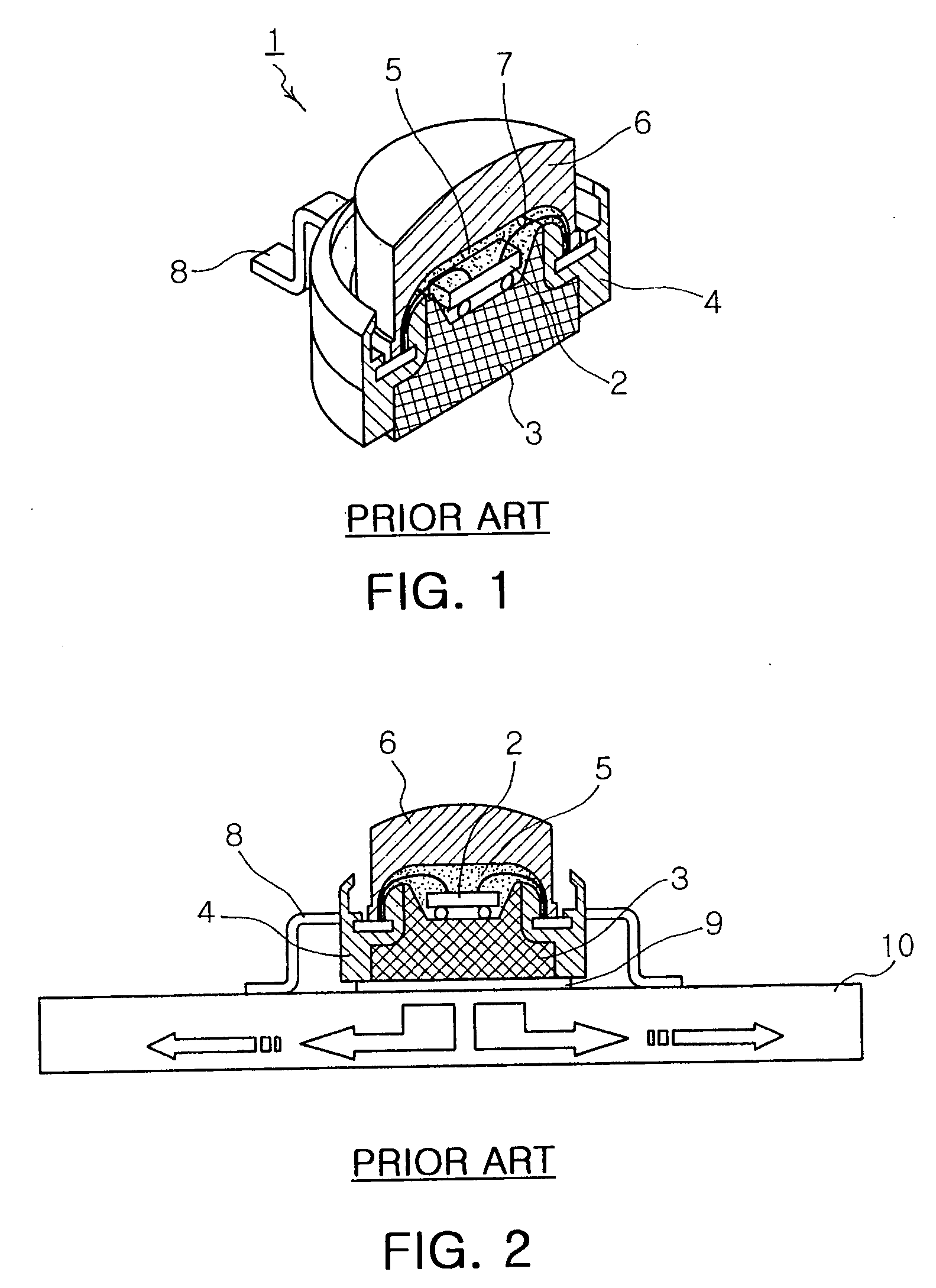
However, the LEDs also fail to cnovert electricity into light for 100%, thereby creating a considerable amount of heat.
As a consequence, the LEDs adopt metal lead frames to radiate heat to the outside because internal components of the LEDs become stressed owing to their thermal expansion coefficient difference if heat is not properly dissipated.
However, the above conventional thermal radiation structure of the LED package has a bulky size thereby to obstruct the miniaturization of an illumination system.
This structure is also complicated obstructing the automation of LED package production as well as requiring a large number of components to be assembled together thereby to burden manufacture cost.

Method used


Image

  • High power light emitting diode package
  • High power light emitting diode package
  • High power light emitting diode package

Examples


first embodiment

[0073]FIG. 7 is a sectional view illustrating the high power LED package 100 according to the present invention with a lens attached thereto. In FIG. 7, the lens 120 is attached to the upper surface of the package body 102 to protect a sealant 110 and the LED chip 112 contained therein. Herein, the lens 120 is generally transferred and formed onto the package body 102, or otherwise fabricated separately and then bonded to the package body 102 with proper means such as an adhesive and the like.

[0074] Structured like this, the first and second sheet metal members 114 and 116 with a simple construction serve as radiating means and terminals, and the integrated package body 102 injection-molded with resin bonds these members strongly, thereby greatly improving thermal radiation efficiency as well as securing excellent robustness while reducing their dimension significantly.

[0075]FIG. 8 is a sectional view illustrating another form of the high power LED package as shown in FIG. 4.

[0076...

second embodiment

[0079]FIG. 9 is a sectional view corresponding to FIG. 4, illustrating a high power LED package according to the present invention, and FIG. 10 is a sectional view illustrating a state in which the LED package of FIG. 9 is mounted on the board.

[0080] Referring first to FIG. 9, the high power LED package 200 of the present embodiment has a construction identical to that of the LED package 100 of the first embodiment, except that a first section 214a of a first sheet metal member 214 is protruded outside from the bottom surface of a package body 202 for a predetermined length. Thus, constitutional elements the same as or similar to those of the LED package 100 are designated with corresponding reference numerals, increased by 100, and detailed description thereof will be omitted.

[0081] When the first section 214a of the first sheet metal member of radiating means are protruded from the bottom surface of the package body 202 as such, it is advantageous when mounting the LED package 20...

third embodiment

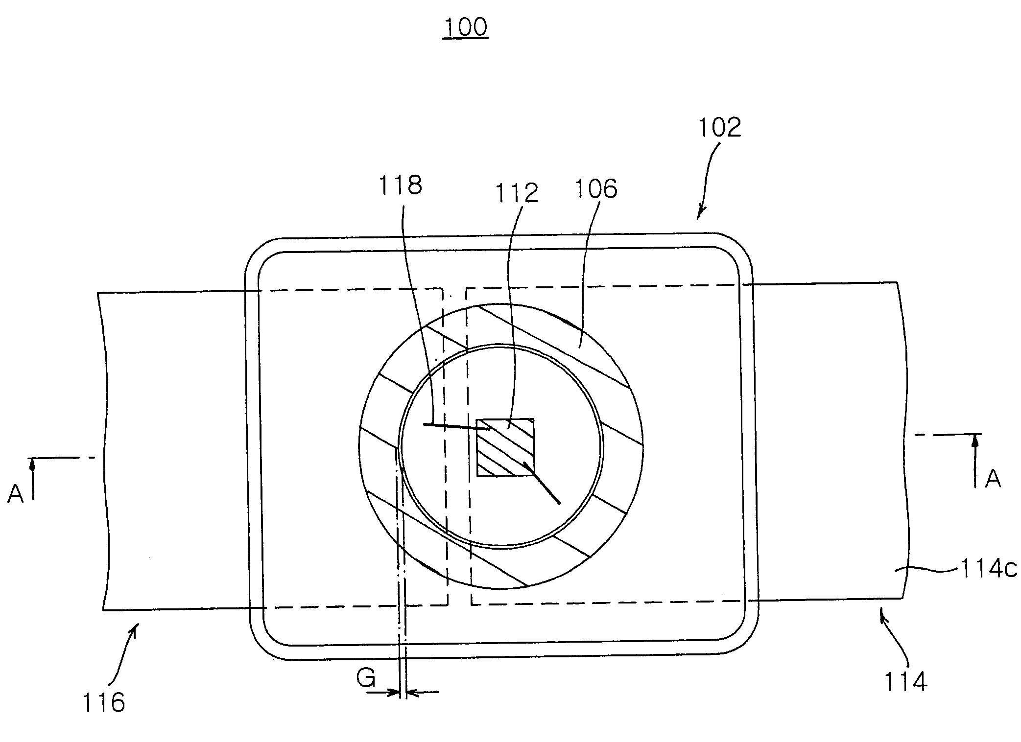
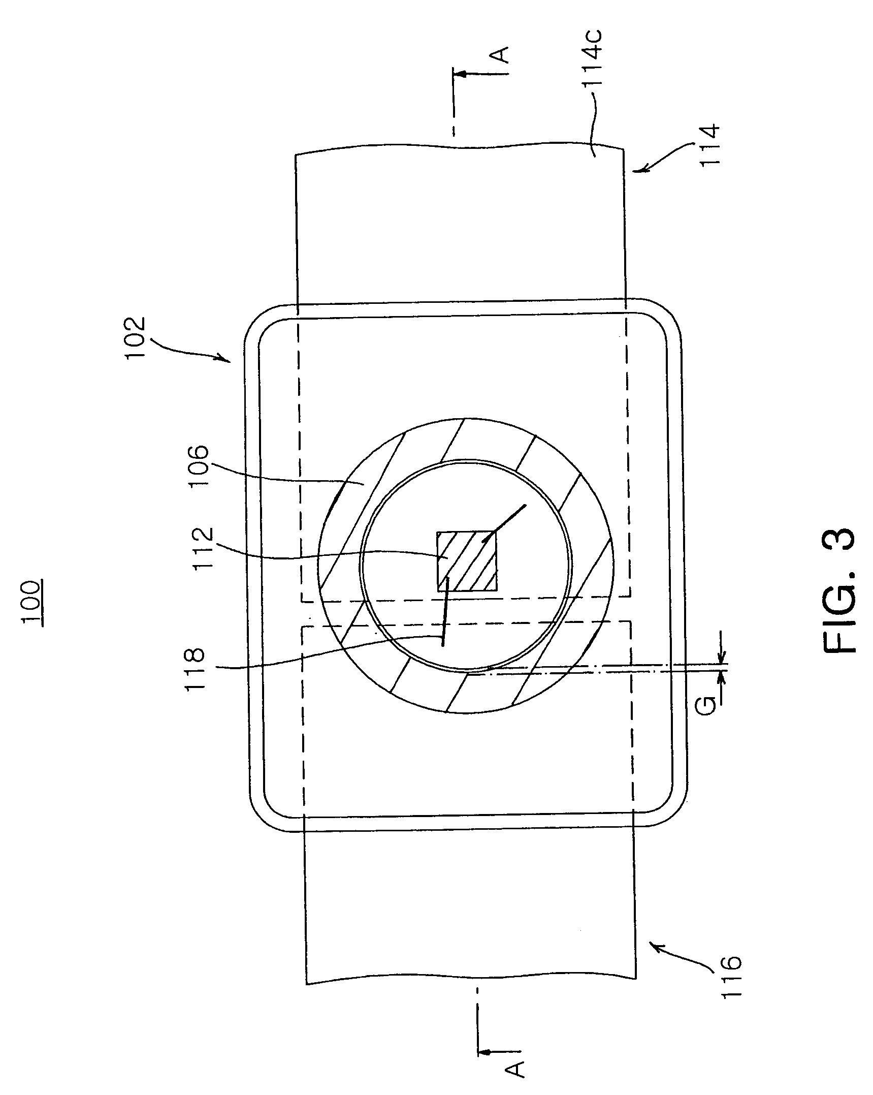
[0084]FIG. 12 is a plan view illustrating a high power LED package according to the present invention, FIG. 13 is a sectional view taken along a line B-B of FIG. 10, and FIG. 14 is a plan view illustrating the high power LED package of FIG. 12 with the upper portion of the package body removed.

[0085] Referring to FIGS. 12 through 14, the LED package 300 according to the third embodiment is discriminated from the LED package 100 according to the first embodiment, in that a first sheet metal member 314 consists of first and second sections 314a and 314b without protruded beyond the side of a package body 302, and a second sheet metal member 316 consists of first and second terminals 316A and 316B. Thus, constitutional elements the same as or similar to those of the LED package 100 are designated with corresponding reference numerals, increased by 200, and detailed description thereof will be omitted.

[0086] According to this embodiment, the first sheet metal member 314 functions as ra...


PUM


Abstract

The invention relates to a high power LED package, in which a package body is integrally formed with resin to have a recess for receiving an LED chip. A first sheet metal member is electrically connected with the LED chip, supports the LED chip at its upper partial portion in the recess, is surrounded by the package body extending to the side face of the package body, and has a heat transfer section for transferring heat generated from the LED chip to the metal plate of the board and extending downward from the inside of the package body so that a lower end thereof is exposed at a bottom face of the package body thus to contact the board. A second sheet metal member is electrically connected with the LED chip spaced apart from the first sheet metal member for a predetermined gap, and extends through the inside of the package body to the side face of the package body in a direction opposite to the first sheet metal member. A transparent sealant is sealingly filled up into the recess. The LED package raises thermal radiation efficiency with a simplified structure in order to reduce the size and thickness thereof.

Description

CLAIM OF PRIORITY [0001] This application claims the benefit of Korean Patent Application Nos. 2004-69730 filed on Sep. 1, 2004 and 2005-37421 filed on May 4, 2005, in the Korean Intellectual Property Office, the disclosures of which are incorporated herein by reference. BACKGROUND OF THE INVENTION [0002] 1. Field of the Invention [0003] The present invention relates to a Light Emitting Diode (LED) package, and more particularly, a high power LED package designed to raise thermal radiation efficiency with a simplified structure in order to reduce the size and thickness thereof. [0004] 2. Description of the Related Art [0005] LEDs are one type of semiconductors, and generate various colors of light when applied with voltage. When each LED generates light, its color is generally determined by chemical ingredients of the LED. Demand for the LEDs is continuously growing since the LEDs have various merits such as long lifetime, low drive voltage, excellent initial drive properties, high ...

Claims


Application Information

Patent Timeline
Patent Type & Authority Applications(United States)
IPC IPC(8): H01L33/00H01L33/64
CPCH01L33/486H01L33/642H01L33/647H01L2224/16245H01L2924/12041H01L24/97H01L2924/1815H01L2224/48091H01L2224/48247H01L2924/00014H01L2924/0002H01L2924/00011H01L2924/00H01L2224/0401H01L33/62H01L33/60
Inventor LEE, SEON GOOKIM, CHANG WOOKHAN, KYUNG TAEG
Owner SAMSUNG ELECTRONICS CO LTD
Learn More