Die anti-tampering sensor

a sensor and sensor circuit technology, applied in the direction of instruments, electrical apparatus casings/cabinets/drawers, semiconductor/solid-state device details, etc., can solve the problems of requiring a substantial about of power dissipation within the integrated circuit, or the prior art protection schemes mentioned are either very complex and difficult to achieve the effect of low power and simple circuit implementation

Inactive Publication Date: 2006-03-02
KARMIC DESIGN USA
View PDF10 Cites 18 Cited by
  • Summary
  • Abstract
  • Description
  • Claims
  • Application Information

AI Technical Summary

Benefits of technology

[0009] It is therefore an object of the present invention to provide a circuit and a method for protecting against tampering of integrated circuits. It is further an object of this invention to provide a low power, simple circuit implementation.

Problems solved by technology

However, the various prior art protection schemes mentioned are either very complex or they require a substantial about of power dissipation within the integrated circuit.

Method used


Image

  • Die anti-tampering sensor
  • Die anti-tampering sensor
  • Die anti-tampering sensor

Examples


Embodiment Construction

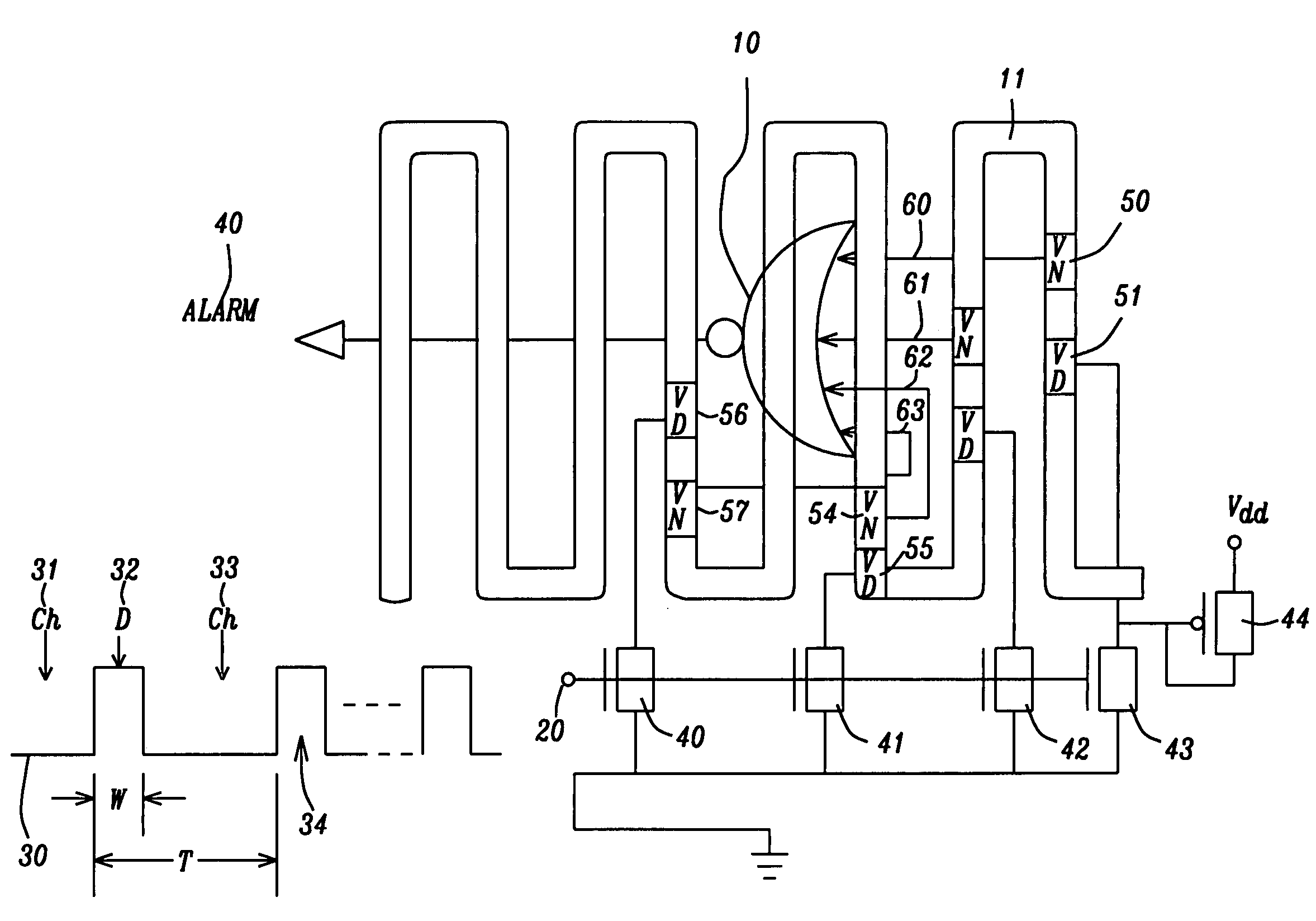
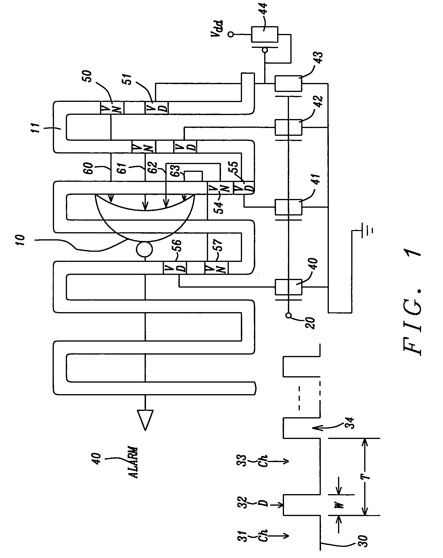
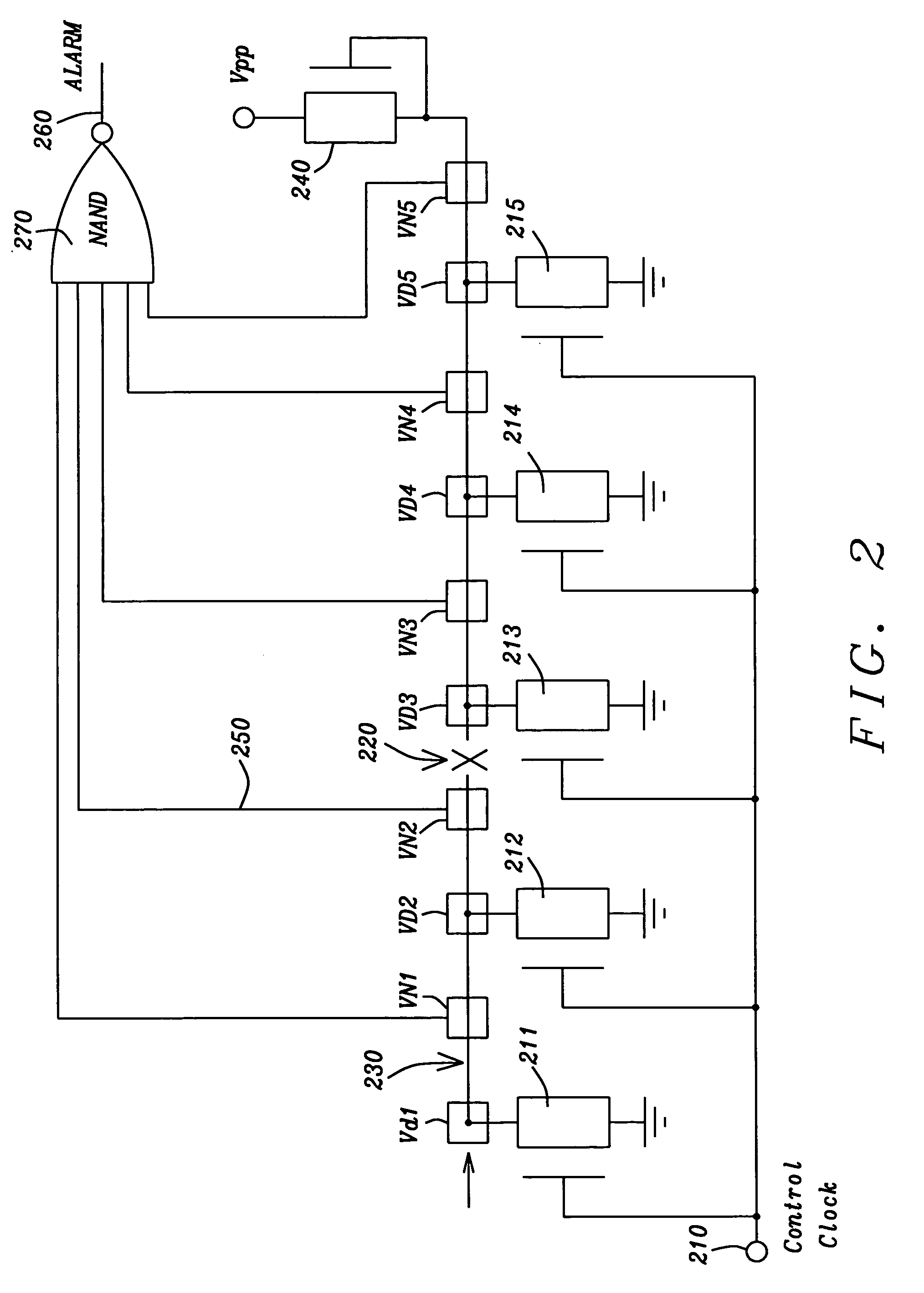
[0017]FIG. 1 shows the main embodiment of this invention. It shows a metal wire loop 11 on top of circuitry in an integrated circuit die. The wire loop is placed over the circuitry or memory, which is to be secured from intrusion. The figure also shows a control clock waveform 30, which feeds the gates of devices 40, 41, 42, 43, and 44.

[0018] The metal wire loop is made up of a metallization layer within the semiconductor die. The loop could also be implemented with polysilicon or other conductive material. The geometry and spacing of the metal wire loop is dictated by the dimensions of the circuit & memory region and by the line widths and spacings and device dimensions within the circuitry to be protected. The fingers of the metal wire loop must be close enough to each other to prevent an unwanted probing or tampering of the circuitry below the metal wire loop.

[0019]FIG. 1 also shows via pairs spaced periodically on the metal wire loop. The figure shows the via pair VD 56 and VN...


PUM


Abstract

This sensor circuit and method for defending against tampering with an integrated circuit die uses metal wire loops to protect the circuitry. In addition, these metal wire loops have several via pairs along its length. One of the vias of the via pair goes to a NAND gate which detects a break in a section of a metal wire loop. A second via of the via pair is used to periodically discharge a metal wire loop to remove residual charge, in preparation for charging the metal wire loop and detecting any uncharged section. A given integrated circuit can have one or more metal wire loops on top of the circuitry to be protected. Each metal wire loop has one or more NAND gates. These outputs of the NAND gates can be fed into OR gates to produce an overall signal which activates an alarm or other security action such as erasure of electrically erasable programmable read only memory (EEPROM).

Description

BACKGROUND OF THE INVENTION [0001] 1. Field of the Invention [0002] The present invention generally relates to the general field of protecting integrated circuits against unwanted intrusion or tampering. More particularly, this invention relates to a sensor circuit and a method, which uses metal wire loops to protect integrated circuit dies from unwanted tampering. [0003] 2. Description of the Prior Art [0004] The circuitry and memory of certain integrated circuits are sensitive and need to be protected from unwanted tampering. Various applications such as automatic teller machines, ATMs, require a high level of protection from external tampering and deciphering of the circuitry and memory. Similarly, pay-per-view television cable boxes require protection against intruders who may attempt to steal cable services by tampering with circuits and memory within the cable boxes. Previous means of protecting circuits include passivation layers covering the sensitive electronic layers. Secu...

Claims


Application Information

Patent Timeline
Patent Type & Authority Applications(United States)
IPC IPC(8): G08B13/14G08B13/26
CPCG06F21/87H01L23/576H01L2924/0002H01L2924/00
Inventor SIN, LIM ENG
Owner KARMIC DESIGN USA
Why Eureka
Try Eureka