Electro-optical device and electronic apparatus

a technology applied in the field of optical devices and electronic devices, can solve the problems of large wiring resistance on the substrate, and achieve the effect of reliable connection to anisotropic conductive sheets

Inactive Publication Date: 2006-03-02
SEIKO EPSON CORP
View PDF5 Cites 16 Cited by
  • Summary
  • Abstract
  • Description
  • Claims
  • Application Information

AI Technical Summary

Benefits of technology

[0011] An advantage of the invention is that it provides an electro-optical device in which a driving circuit element and a FPC can be connected on a substrate by use of an ACF extending over a driver IC chip and the FPC.
[0012] According to an aspect of the invention, an electro-optical device that displays an image on a display region on the substrate based on input signals, includes a driving circuit element that has a plurality of electrode sections; a flexible printed board that has a plurality of first wiring lines; and an anisotropic conductive sheet that is formed to extend across the driving circuit element and the flexible printed board on the substrate and in which the plurality of electrode sections are electrically connected to a plurality of second wiring lines on the substrate, respectively, and the plurality of first wiring lines are electrically c...

Problems solved by technology

When the distance between the driver IC chip and the FPC becomes large, t...

Method used


Image

  • Electro-optical device and electronic apparatus
  • Electro-optical device and electronic apparatus
  • Electro-optical device and electronic apparatus

Examples


Embodiment Construction

[0028] Hereinafter, a liquid crystal display panel as an electro-optical device according to an embodiment of the invention will be described with reference to the drawings. The liquid crystal display panel according to the present embodiment may be a passive-type panel such as an STN or may be an active-type panel such as a TFD, a TFT, or an LTP.

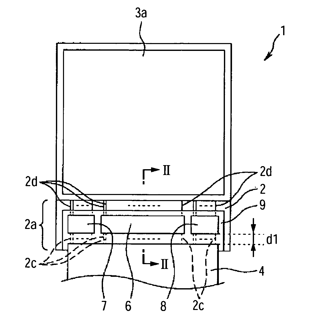
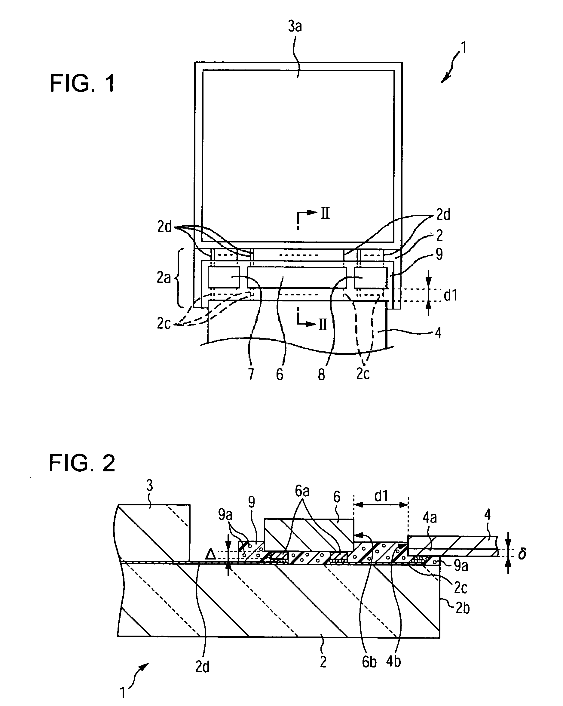
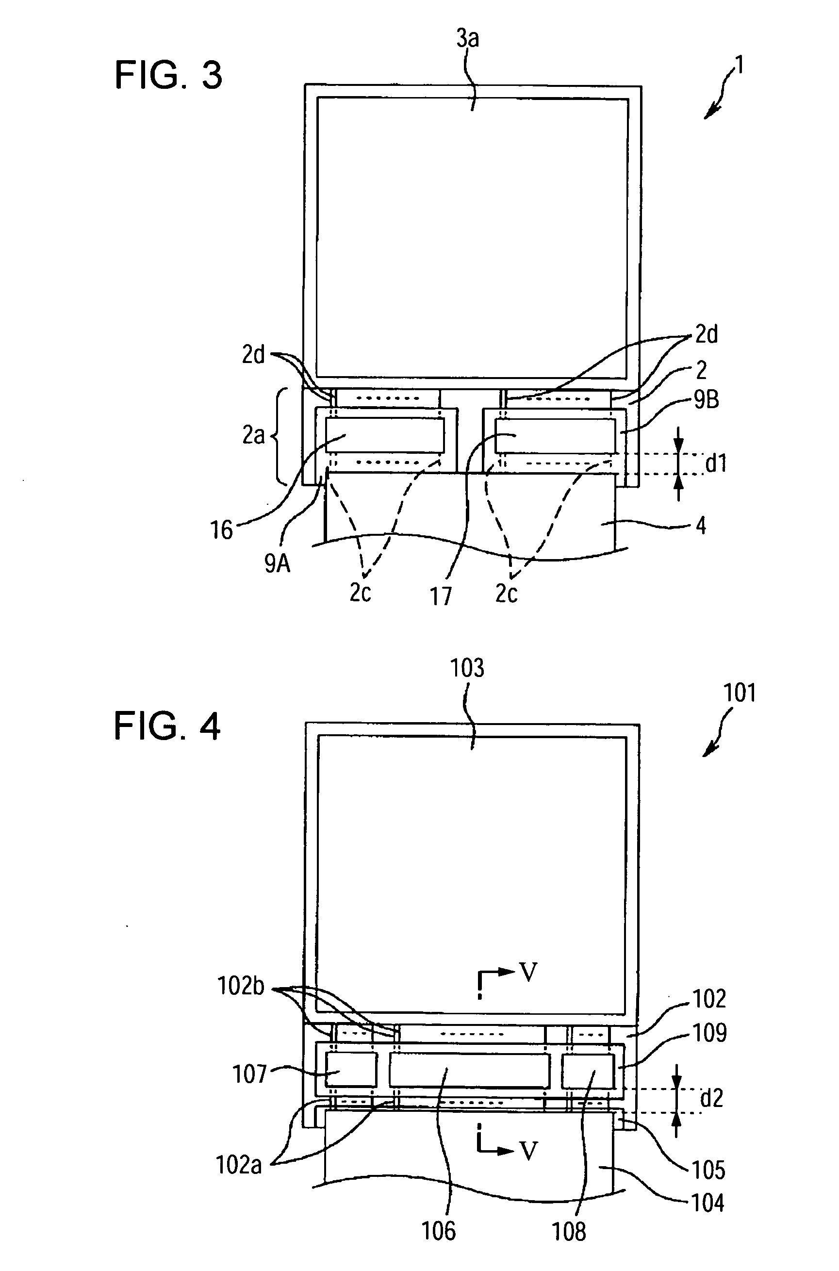
[0029]FIG. 1 is a plan view explaining a configuration of the liquid crystal panel according to an embodiment of the invention. FIG. 2 is a cross-sectional view of the liquid crystal panel taken along the line II-II of FIG. 1.

[0030] The liquid crystal panel 1 is constituted by bonding two glass substrates 2 and 3 to each other. Between the bonded two glass substrates, liquid crystal is sealed. A region where the liquid crystal is sealed constitutes a display region 3a as a display section, on which an image is displayed.

[0031] Between two substrates, one glass substrate 2 has a larger area than the other glass substrate 3. Therefore, in ...


PUM


Abstract

An electro-optical device that displays an image on a display region on a substrate based on an input signal, includes a driving circuit element that has a plurality of electrode sections; a flexible printed board that has a plurality of first wiring lines; and an anisotropic conductive sheet that is formed to extend across the driving circuit element and the flexible printed board on the substrate and in which the plurality of electrode sections are electrically connected to a plurality of second wiring lines on the substrate, respectively, and the plurality of first wiring lines are electrically connected to the plurality of second wiring lines, respectively.

Description

BACKGROUND OF THE INVENTION [0001] 1. Technical Field [0002] The present invention relates to electro-optical devices and to electronic apparatuses, and more specifically, to an electro-optical device having a driving circuit element mounted on a substrate and a flexible printed board connected to the substrate and to an electronic apparatus. [0003] 2. Related Art [0004] Conventionally, electro-optical devices such as liquid crystal devices have been widely mounted on an electronic apparatus such as a cellular phone, a projector or the like. [0005] A liquid crystal display panel having a two-dimensional-matrix-type liquid crystal display region is generally driven by a driving semiconductor device, such as a driver IC chip so as to generate an image by a transmitted light component and a reflected light component to display on the display region. The driver IC chip serving as a driving circuit element is mounted on the substrate of a liquid crystal panel by using an ACF (anisotropic...

Claims


Application Information

Patent Timeline
IPC IPC(8): G02F1/1345
CPCG02F1/13452G02F2001/13456H05K2201/10674H05K3/361H05K3/323G02F1/13456G02F1/1345
Inventor NAKAZAWA, MASAHIKO
Owner SEIKO EPSON CORP
Why Eureka
Try Eureka