

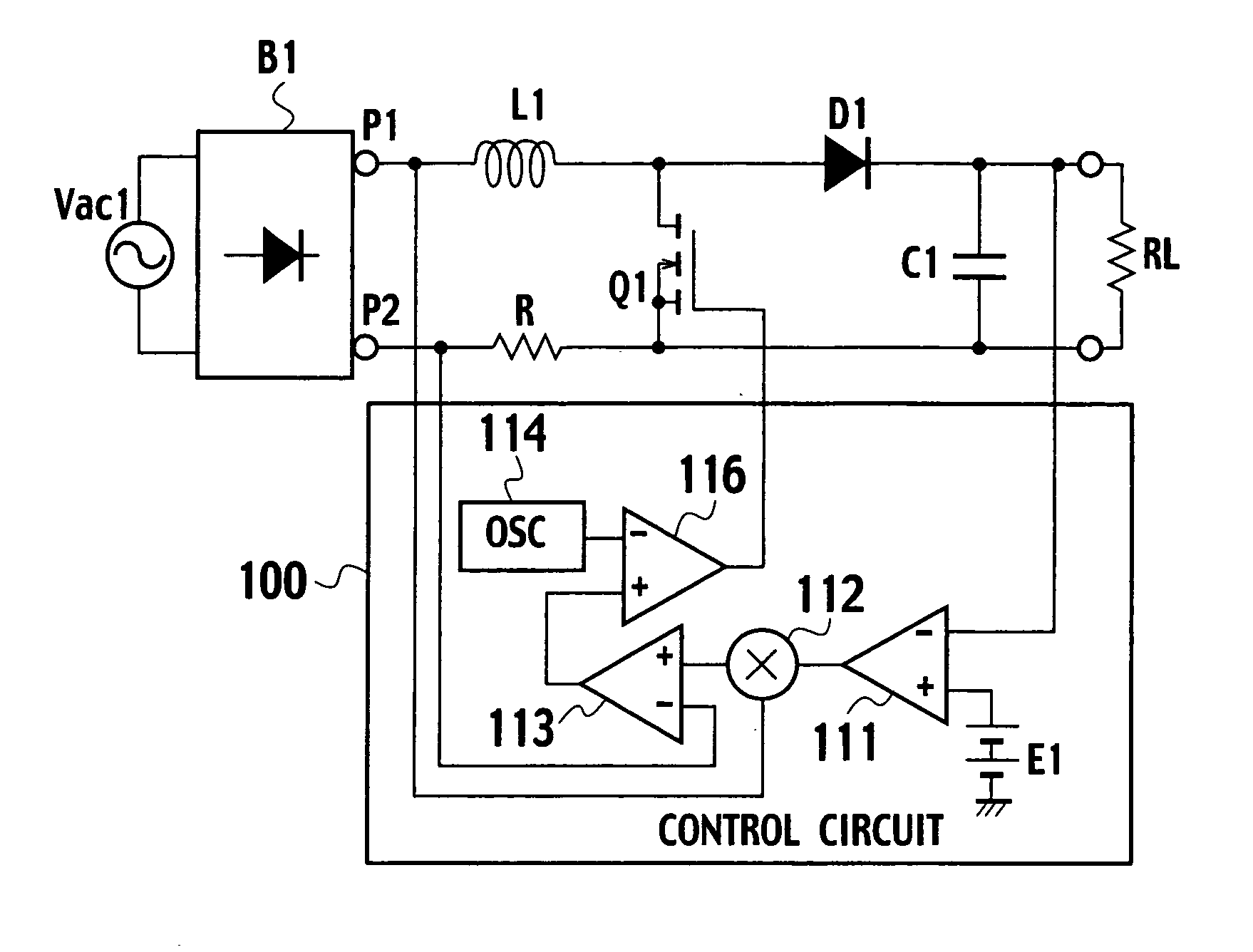
Power factor improving circuit
- Summary
- Abstract
- Description
- Claims
- Application Information
AI Technical Summary
Benefits of technology
Problems solved by technology
Method used
Image

Examples
embodiment 1
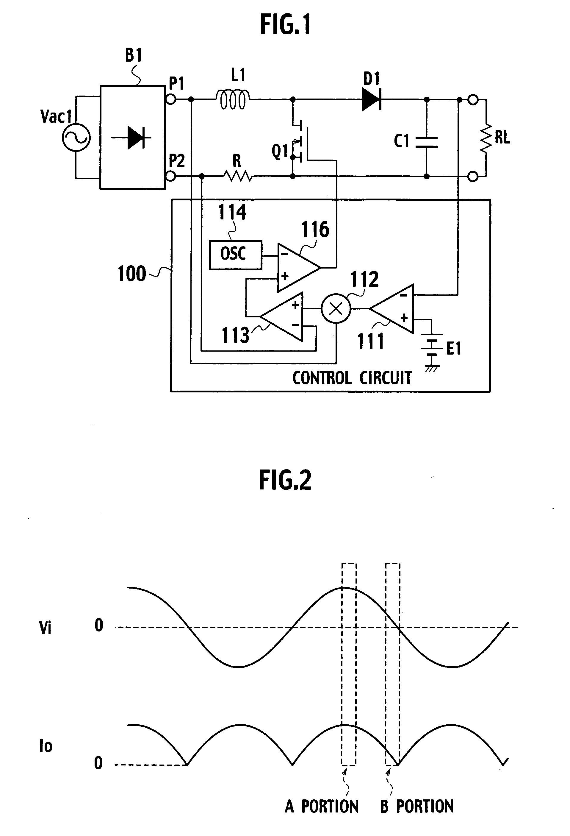
[0048]FIG. 5 is a circuit configuration diagram illustrating a power factor improving circuit according to Embodiment 1. FIG. 6 is a timing chart illustrating each of an input current waveform and a switching frequency of the power factor improving circuit according to Embodiment 1. FIG. 6 shows that the switching frequency f of the main switch Q1 changes form zero to, for example, 100 kHz when input current Ii changes from zero to a maximum value.
[0049] In Embodiment 1, when the input current is a lower limit setting current or less, the switching frequency of the main switch is set to a lower limit frequency (for example, 20 kHz). When the input current is an upper limit setting current or more, the switching frequency of the main switch is set to an upper limit frequency (for example, 100 kHz). When the input current ranges from the lower limit setting current to the upper limit setting current, the switching frequency of the main switch is gradually changed from the lower limit...
embodiment 2
[0078]FIG. 13 is a timing chart of a switching frequency that is changed according to an input current waveform and voltage input to a VCO in a power factor improving circuit according to Embodiment 2.
[0079] In Embodiment 1 shown in FIG. 10, when the input current Ii reached the low current portion, the switching frequency f of the main switch Q1 was set to the lower limit frequency fl2 (for example, 20 kHz) by the VCO 115. In Embodiment 2 shown in FIG. 13, when the input current Ii is in the low current portion, the operation of the main switch Q1 is stopped by the VCO 115 in the case of the lower limit frequency fl2. At a portion where the operation is stopped, since the amount of the AC power supply current is small, distortion of the input current waveform is suppressed to a minimum.
embodiment 3
[0080] In Embodiment 3, when the voltage, which is proportional to the input current, is the setting voltage or less, the switching frequency of the main switch is set to the lower limit frequency (for example, 20 kHz), and when the voltage, which is proportional to the input current, exceeds the setting voltage, the switching frequency of the main switch is set to the upper limit frequency (for example, 100 kHz).
[0081]FIG. 14 is a specific circuit configuration diagram of VCO of a power factor improving circuit according to Embodiment 3. In VCO 115 shown in FIG. 14, a resistor Ri is connected to a negative-side output terminal P2 of a full-wave rectifier circuit B1 and a resistor R2 is connected to the resistor Ri in series. A comparator 115b inputs voltage of a junction of the resistor RI and the resistor R2 to a +terminal and a reference voltage Erl to a terminal. The comparator 115b outputs an H-level voltage to a base of a transistor TR1 when the voltage at the junction of the...
PUM
 Abstract
Description
Claims
Application Information