Eureka AIR delivers breakthrough ideas for toughest innovation challenges, trusted by R&D personnel around the world.

Semiconductor storage apparatus

Active Publication Date: 2006-03-02
KIOXIA CORP
View PDF4 Cites 0 Cited by
  • Summary
  • Abstract
  • Description
  • Claims
  • Application Information

AI Technical Summary

Benefits of technology

[0024] a connection switching circuit which connects electrically the pair of bit lines and the pair of sense nodes when a write control signal is in a prescribed logic level; and
[0025] a timing control circuit which

Problems solved by technology

As for the conventional one transistor—one capacitor DRAM cell including a trench capacitor or a stacked capacitor, there is a concern that its fabrication may become difficult as it becomes finer.
However, holes are stored in the body having a low potential.
Practically, if the word line WL is subjected to pumping approximately 500 times, then the readout margin for the data “1” is lost and the risk that a fail may occur becomes high.
Furthermore, such a sense amplifier circuit has a problem of a poor efficiency in the refresh operation as well.
In addition, there is also a problem that the number of cells that can be accessed is limited when conducting fast column access.
If time required for FBC writing is longer than the cycle time when writing data by using fast column access, then a write fail occurs and this results in a problem that the column access cycle time cannot be made shorter than the FBC write time.

Method used


Image

  • Semiconductor storage apparatus
  • Semiconductor storage apparatus
  • Semiconductor storage apparatus

Examples


Embodiment Construction

[0034] Hereafter, an embodiment of the present invention will be described with reference to the drawings.

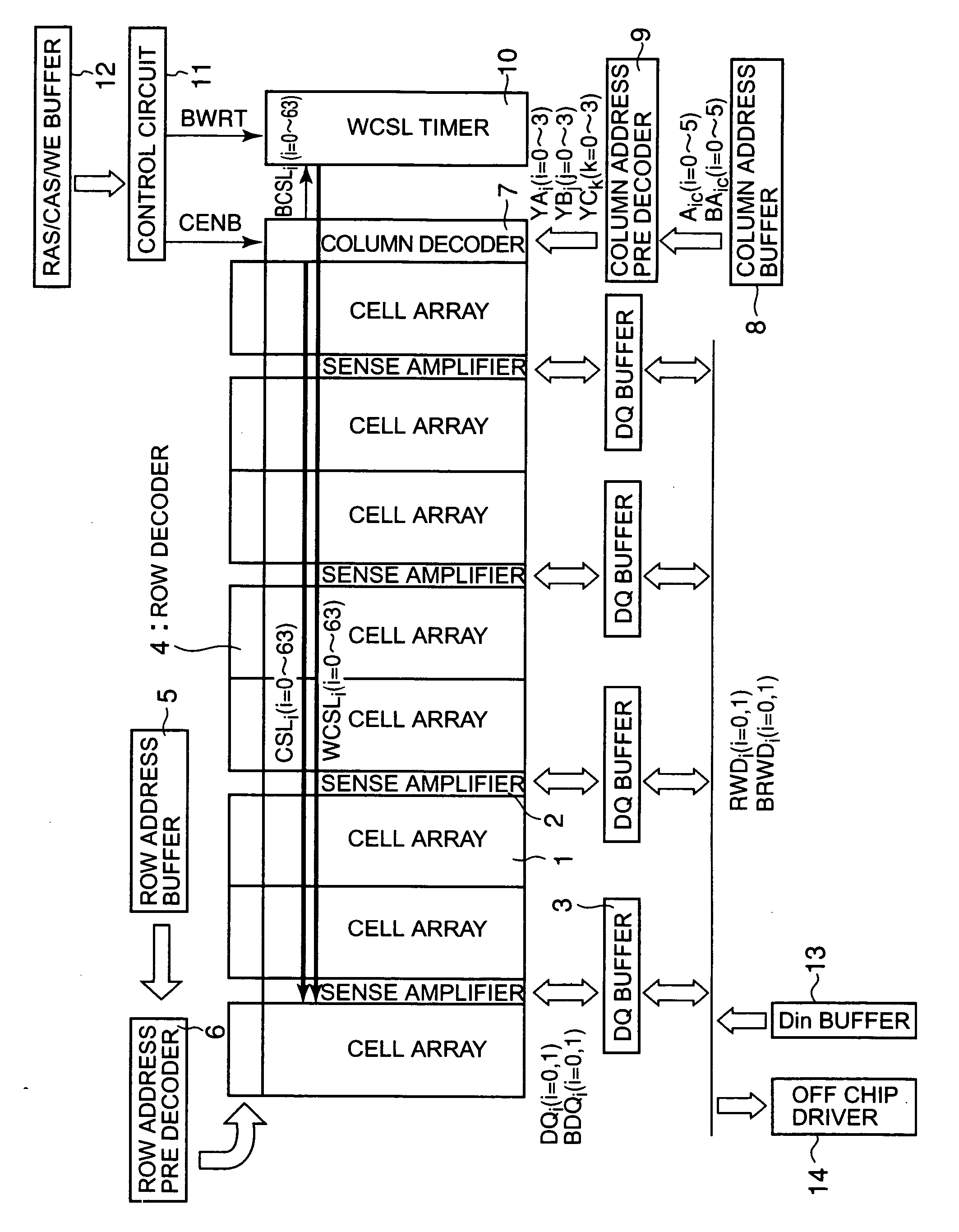
[0035]FIG. 1 is a block diagram showing a general configuration of a semiconductor storage apparatus according to an embodiment of the present invention. The semiconductor storage apparatus shown in FIG. 1 includes a plurality of cell arrays 1 arranged in a row direction, sense amplifiers 2 disposed between these cell arrays 1, DQ buffers 3 for conducting input / output for data line, row decoders 4, a row address buffer 5, a row address pre-decoder 6, a column decoder 7, a column address buffer 8, a column address pre-decoder 9, a WCSL timer 10 described later, a control circuit 11, a RAS / CAS / WE buffer 12, a Din buffer 13, and an off-chip driver 14.

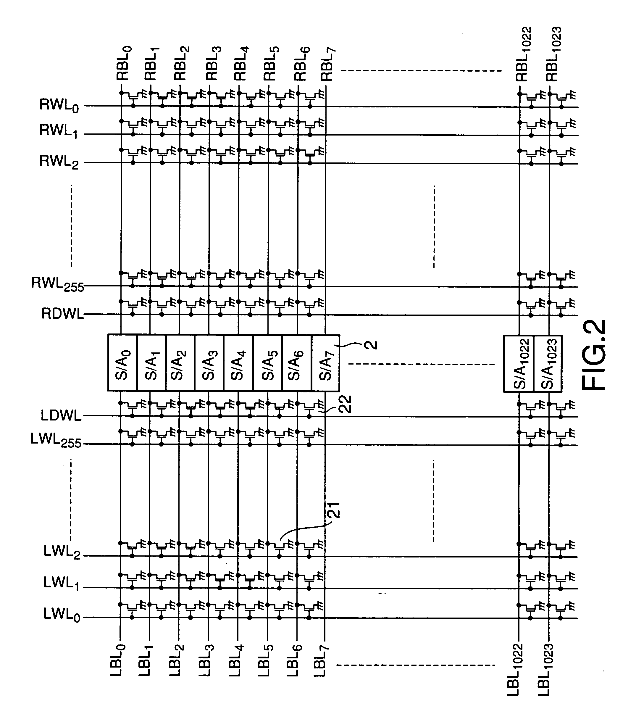
[0036]FIG. 2 is a circuit diagram showing an example of a detailed configuration of the cell array 1 and the sense amplifiers 2 (S / A0 to S / A1023). As shown in FIG. 2, 256 word lines LWL0 to LWL255, a dummy word line LDWL, 256 word li...


PUM


Abstract

A semiconductor storage apparatus according to one embodiment of the present invention, comprising: a cell array including a plurality of memory cells, each being connected to bit lines and word lines arranged in a row direction and a column direction; and a sense amplifier which controls read-out of data stored in the memory cells, wherein the sense amplifier includes: a pair of sense nodes provided corresponding to a pair of the bit lines; a connection switching circuit connected between the pair of bit lines and the pair of sense nodes, which connects electrically the pair of bit lines and the pair of sense nodes when a write control signal is in a prescribed logic level; and a timing control circuit which sets the write control signal to the prescribed logic level substantially at the same time as a timing when a column selection signal selects a column to which the memory cell to be written is connected during data writing period for the memory cells, and holds the write control signal to the prescribed logic level during a first period regulated by the timing when the column selection signal selects the columns.

Description

CROSS REFERENCE TO RELATED APPLICATIONS [0001] This application is based upon and claims the benefit of priority from the prior Japanese Patent Application No. 2004-253059, filed on Aug. 31, 2004, the entire contents of which are incorporated herein by reference. BACKGROUND OF THE INVENTION [0002] 1. Field of the Invention [0003] The present invention relates to a semiconductor storage apparatus including cell arrays having a plurality of memory cells, and sense amplifiers. [0004] 2. Related Art [0005] As for the conventional one transistor—one capacitor DRAM cell including a trench capacitor or a stacked capacitor, there is a concern that its fabrication may become difficult as it becomes finer. As a candidate for a future DRAM, a new memory cell FBC (Floating Body Cell) is proposed (see Japanese Patent Application Laid-Open Publication Nos. 2003-68877 and 2002-246571). In the FBC, majority carriers are stored in a floating body of an FET (Field Effect Transistor) formed on SOI (Si...

Claims


Application Information

Patent Timeline
IPC IPC(8): G11C7/00
CPCG11C7/06G11C7/22G11C2207/065G11C11/4091G11C2207/005G11C11/4076
Inventor OHSAWA, TAKASHI
Owner KIOXIA CORP
Why Eureka
Eureka Blog
Learn More