Method for manufacturing piezoelectric resonator

a piezoelectric resonator and manufacturing method technology, applied in the direction of piezoelectric/electrostrictive transducers, generators/motors, transducer types, etc., can solve the problems of low frequency concentration, inability to accurately adjust the frequency, and difficulty in accurately positioning the etching resist ink or the metallic mask

Active Publication Date: 2006-03-09
MURATA MFG CO LTD
View PDF9 Cites 6 Cited by
  • Summary
  • Abstract
  • Description
  • Claims
  • Application Information

AI Technical Summary

Benefits of technology

[0015] In order to overcome the problems described above, preferred embodiments of the present invention provide a method for manufacturing a piezoelectric resonator including very small vibration electrodes in which frequencies can be adjusted accurately without the need for a complicated positioning operation.

Problems solved by technology

In this method, however, variations in the application quantity of ink are large, and the concentration of the frequency is low, thereby failing to adjust the frequency accurately.
However, in either of the method for using etching resist ink or a metallic mask, it is difficult to accurately position the etching resist ink or the metallic mask to the vibrating electrodes, thereby making the frequency adjustment difficult.
In this case, a slight deviation of etching resist ink or a metallic mask seriously influences the adjustment precision.
In contrast, if there is a deviation 6 of the metallic thin film 61 from the vibrating electrode 60, as shown in FIG. 13B, the resulting vibrating electrode has a thicker portion and a thinner portion, i.e., the thickness of the resulting vibrating electrode is not uniform, thereby making it difficult to adjust the frequency to be a target frequency.
The adjusting method disclosed in Japanese Unexamined Patent Application Publication No. 6-224677 presents the following problems since the first formation of a film for electrodes is performed on the overall surface of the piezoelectric substrate.
One problem is that trapping of piezoelectric vibration becomes insufficient when measuring the frequency, and thus, a spurious response is generated, thereby making it difficult to accurately measure the frequency.
The other problem is that, since the film deposition area is large, the temperature of the piezoelectric substrate becomes higher if film deposition is performed by sputtering, thereby encouraging the depolarization.

Method used


Image

  • Method for manufacturing piezoelectric resonator
  • Method for manufacturing piezoelectric resonator
  • Method for manufacturing piezoelectric resonator

Examples


first preferred embodiment

[0051] A manufacturing process of a piezoelectric resonator according to a first preferred embodiment of the present invention is shown in FIGS. 1A through 4B. The piezoelectric resonator of this preferred embodiment is a bi-terminal resonator.

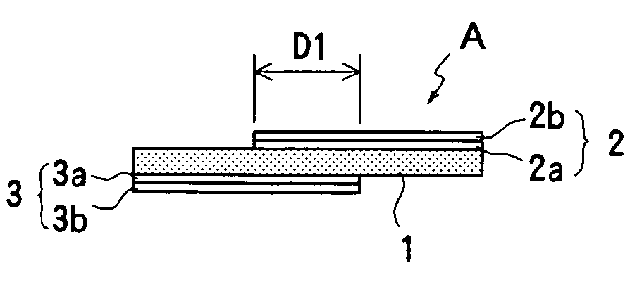
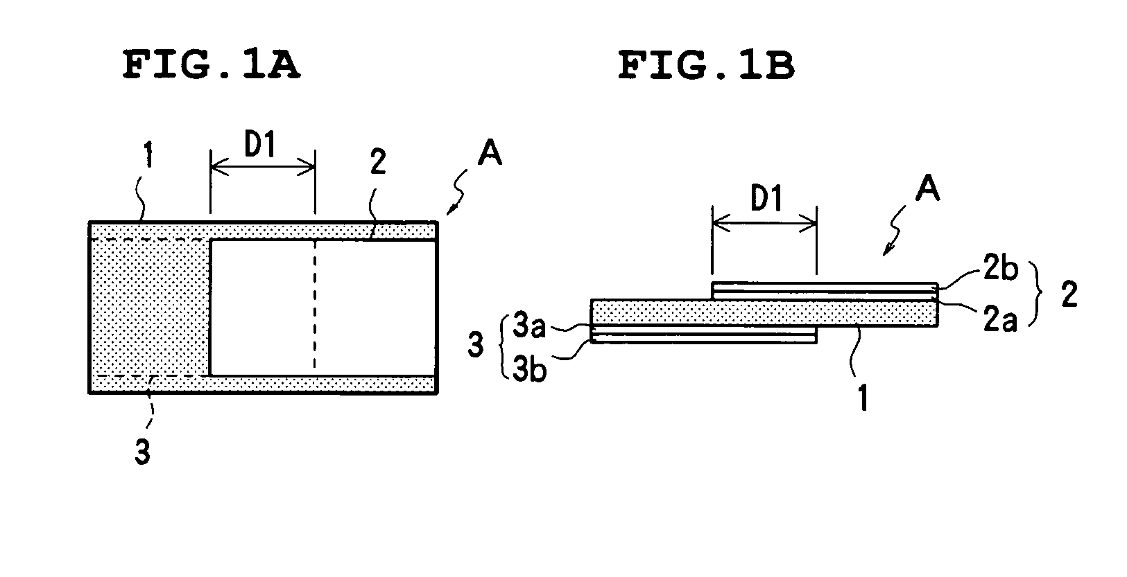
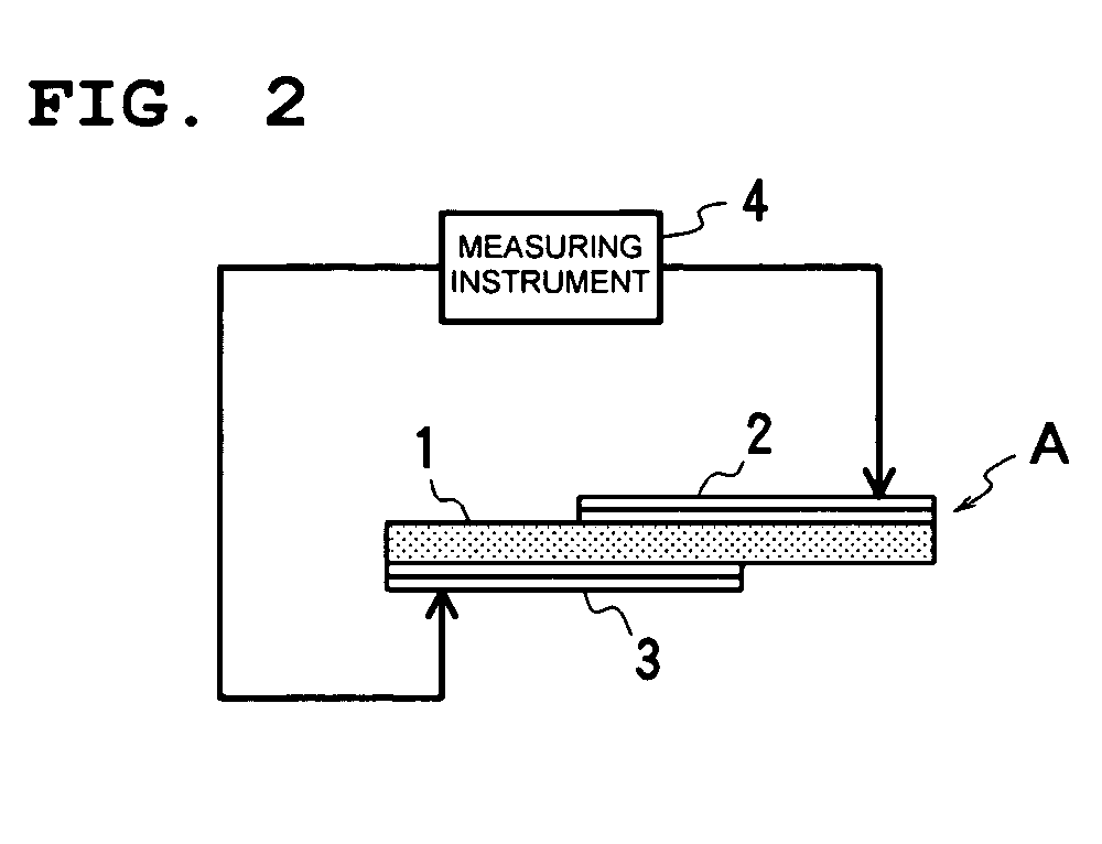
[0052] In FIGS. 1A and 1B, a resonator A in the first stage of the manufacturing process is shown. The resonator A includes a substantially rectangular piezoelectric substrate 1, and first electrodes 2 and 3 are respectively formed on the obverse and reverse surfaces of the piezoelectric substrate 1. The resonator A is preferably an energy-trap thickness-shear vibration mode resonator, and polarization has been performed on the obverse and reverse surfaces of the piezoelectric substrate 1 in the parallel direction. One end of the first electrode 2 and one end of the first electrode 3 oppose each other at an approximately central portion of the piezoelectric substrate 1, and the other ends thereof are led out to different terminals. An opposin...

second preferred embodiment

[0063] A manufacturing process of a piezoelectric resonator according to a second preferred embodiment of the present invention is shown in FIGS. 5A through 8C. The piezoelectric substrate of this preferred embodiment is preferably a tri-terminal filter. FIGS. 5A, 5B, and 6 are similar to FIGS. 1A, 1B, and 2, respectively, and elements in FIGS. 5A, 5B, and 6 similar to those in FIGS. 1A, 1B, and 2 are indicated by like reference numerals, and an explanation thereof is thus omitted.

[0064]FIGS. 7A and 7B illustrate a resonator B1 in the second stage. On the obverse surface of the resonator B1, a second electrode 20 is formed from the opposing portion D1 of the resonator A of the first stage to the end of the piezoelectric substrate 1 opposite to the side on which the first electrode 2 is disposed. On the reverse surface of the resonator B1, a second electrode 21 is formed from the opposing portion D1 of the resonator A of the first stage to the end of the piezoelectric substrate 1 op...

third preferred embodiment

[0071] A manufacturing process of a piezoelectric resonator according to a third preferred embodiment of the present invention is shown in FIGS. 9A through 12C. The piezoelectric resonator is preferably a two-stage double-mode filter obtained by forming two tri-terminal filters on a single piezoelectric substrate.

[0072]FIGS. 9A and 9B illustrate a resonator A2 in the first stage. The resonator A2 includes a substantially rectangular piezoelectric substrate 31, and polarization has been performed on the obverse and reverse surfaces of the piezoelectric substrate 1 in the parallel direction. A first electrode 32 is formed at an approximately central portion of the obverse surface of the piezoelectric substrate 31, while first electrodes 33 and 34 are formed at two ends of the reverse surface of the piezoelectric substrate 31. The first electrode 32 on the obverse surface opposes the first electrodes 33 and 34 on the reverse surface at the two portions of the piezoelectric substrate 3...


PUM

PropertyMeasurementUnit
frequencyaaaaaaaaaa
thicknessaaaaaaaaaa
cohesionaaaaaaaaaa

Abstract

A method of manufacturing a piezoelectric resonator includes forming first electrodes larger than vibrating electrodes in an area D1 including the vibrating electrodes on obverse and reverse surfaces of a piezoelectric substrate, and measuring the resonant frequency fr1 of a resonator including the first electrodes. The thickness of a metallic thin film required for frequency adjustment is determined based on the measured resonant frequency. Then, second electrodes formed of the metallic thin film having the determined thickness are formed in an area D2 including at least the vibrating electrodes of the piezoelectric substrate. By removing unnecessary portions of the first and second electrodes, a pattern of the resulting vibrating electrodes is formed. Thus, high-accuracy frequency adjustment can be achieved without the need for complicated positioning.

Description

BACKGROUND OF THE INVENTION [0001] 1. Field of the Invention [0002] The present invention relates to a method for manufacturing a piezoelectric resonator in which vibrating electrodes are disposed on both surfaces of a piezoelectric substrate and piezoelectric vibration is trapped between the vibrating electrodes, and more particularly, the present invention relates to a method for adjusting the frequency of the piezoelectric resonator. [0003] 2. Description of the Related Art [0004] In recent years, in the field of piezoelectric resonators used in, for example, oscillators or filters, there is an increasing demand for accurately adjusting the frequency. Previously, ink is applied onto an electrode, and the frequency is adjusted by a mass load of the electrode. In this method, however, variations in the application quantity of ink are large, and the concentration of the frequency is low, thereby failing to adjust the frequency accurately. [0005] To solve this problem, Japanese Unexa...

Claims


Application Information

Patent Timeline
Patent Type & Authority Applications(United States)
IPC IPC(8): H04R17/00H03H3/04H03H9/02
CPCH03H3/04H03H9/131H03H9/132H03H9/177H03H9/56Y10T29/49128H04R17/10Y10T29/4913Y10T29/49135Y10T29/49156Y10T29/42H03H2003/0428
Inventor MORIMURA, TETSUYAIKEDA, YOSHIHIROIRIE, MAKOTOMATSUSHITA, MOTONORI
Owner MURATA MFG CO LTD
Why Eureka
Try Eureka