Method for fabricating conductive bump of circuit board

a circuit board and bump technology, applied in resist details, printed circuit aspects, semiconductor/solid-state device details, etc., can solve the problems of reducing the reliability of fabrication, unable to reduce the cost of stencil fabrication, and difficult to allow solder material to pass through the stencil opening, etc., to achieve the effect of improving fabrication reliability

Active Publication Date: 2006-03-09
PHOENIX PRECISION TECH CORP
View PDF1 Cites 17 Cited by
  • Summary
  • Abstract
  • Description
  • Claims
  • Application Information

AI Technical Summary

Benefits of technology

[0012] According to the foregoing method for fabricating conductive bumps of a circuit board proposed in the present invention, the conductive layer serving as a current conductive path for a subsequent electroplating process is firstly formed on any surface of the circuit board. Then, the patterned resist layer is formed on the other surface of the circuit board, such that the conductive bump is formed on the conductive pad exposed from the patterned resist layer by an electroplating process via the conductive layer. Subsequently, another patterned resist layer is formed on the conductive layer, and the conductive bump is formed on the conductive pad covered by the conductive layer by an electroplating process. Therefore, the conductive bumps can be successively formed on the conductive pads located on different surfaces of the circuit board for electrically connecting the exterior. Furthermore, the present invention can employ an electroplating process in place of a prior-art printing method to form the conductive bump of the circuit board, so as to improve fabrication reliability.

Problems solved by technology

Thus, a cost of stencil fabrication cannot be reduced due to difficulties in performing mold opening of the stencil.
Also, it is difficult to allow the solder material to pass through the opening of the stencil due to smallness of the opening.
Therefore, the stencil has to be wiped out after performing a certain number of printings to ensure the cleanness of the stencil during practical operation, otherwise the shape and dimension of the solder material might be altered to cause an inconvenience as well as a decreased reliability in fabrication.

Method used


Image

  • Method for fabricating conductive bump of circuit board
  • Method for fabricating conductive bump of circuit board
  • Method for fabricating conductive bump of circuit board

Examples


Embodiment Construction

[0017] A method for fabricating conductive bumps of a circuit board proposed in the present invention can be more fully understood by reading the detailed description of the preferred embodiments. What needs to be concerned here is that the drawings are simplified schematic diagrams, and thus only constructs relevant to the present invention are illustrated. Also, these constructs are not drawn according to actual amounts, shapes and dimensions. Actually, the amount, shape and dimension are an optional design and the arrangements of the constructs may be very complex in the reality.

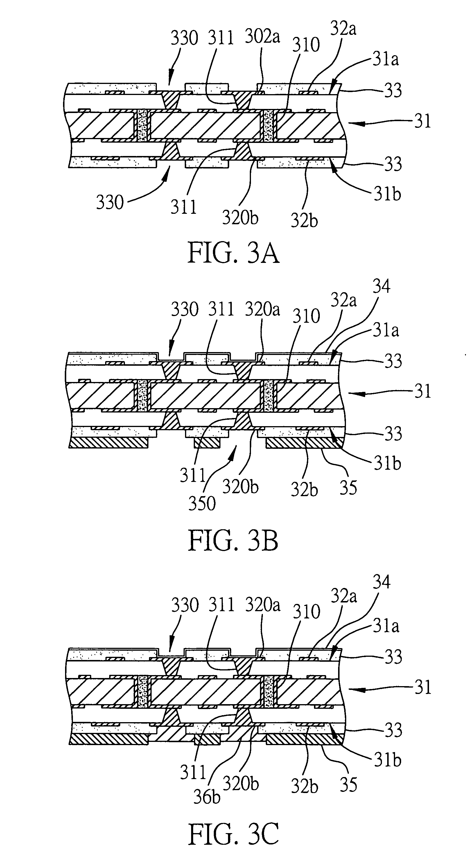
[0018]FIG. 3A to FIG. 3G are cross-sectional views of a method for fabricating conductive bumps of a circuit board according to the present invention.

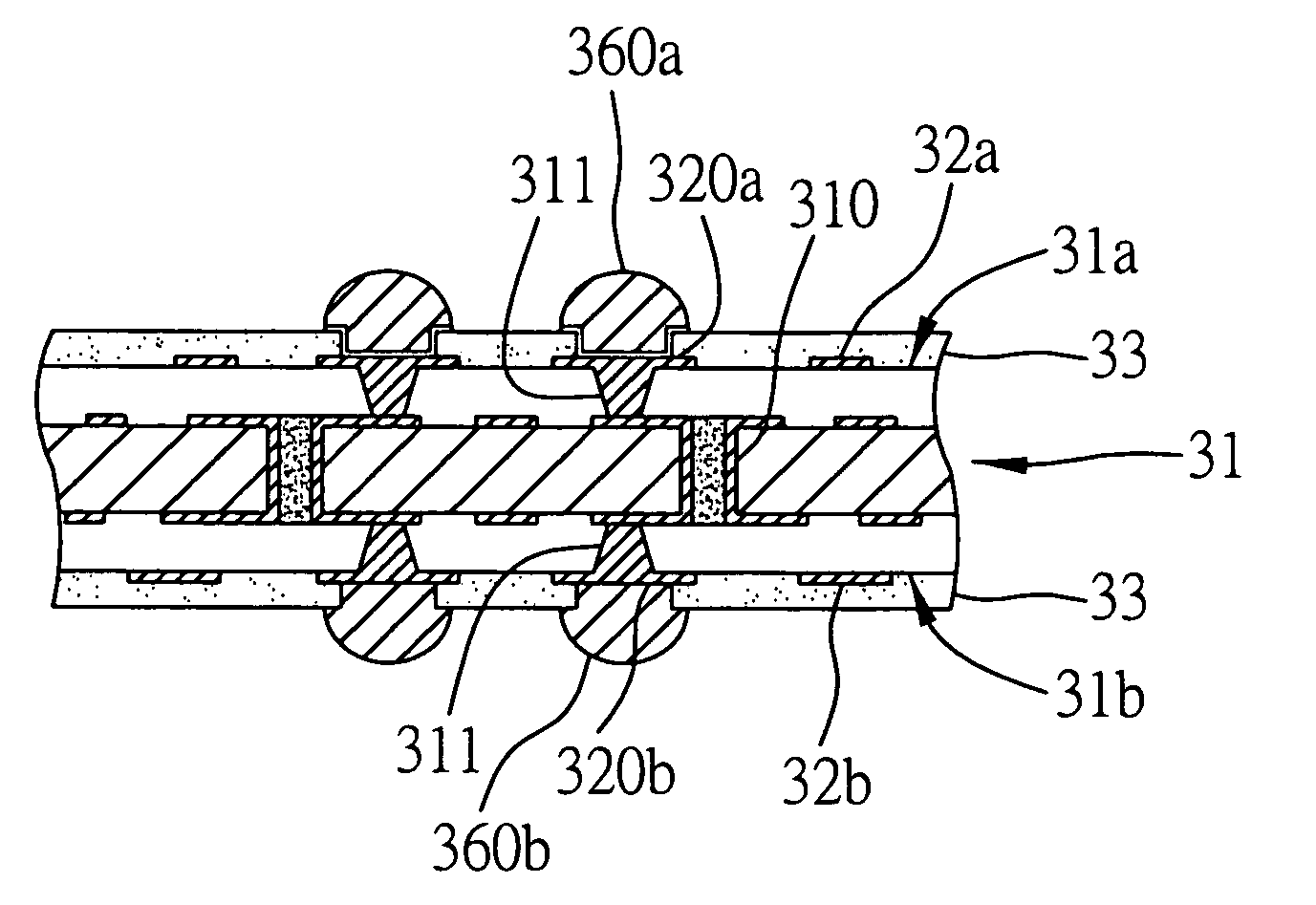
[0019] Referring to FIG. 3A, first of all, a circuit board 31 having a first surface 31a and a corresponding second surface 31b is provided. A circuit structure 32a having a plurality of conductive pads 320a and a circuit structure 32b having a plurality o...


PUM


Abstract

A method for fabricating conductive bumps of a circuit board is proposed. First of all, a circuit board having a first surface and a corresponding second surface is provided. A circuit structure having a plurality of conductive pads is formed on each of the first surface and the second surface, and conductive structures are formed in the circuit board for electrically connecting the circuit structures. Also, an insulating layer having a plurality of openings penetrating therethrough is formed on the circuit board for exposing the conductive pad. Then, a conductive layer is formed on a surface of the insulating layer having the opening formed on the first surface of the circuit board. An electroplating process is performed via the conductive layer and the conductive structure, such that a conductive bump is formed on the conductive pad located on the second surface of the circuit board. Subsequently, a resist layer is formed on the second surface of the circuit board to cover the conductive bump, and another resist layer having openings penetrating therethrough is formed on the first surface of the circuit board to expose the conductive pad. Finally, a conductive bump is formed on the conductive pad located on the first surface of the circuit board by an electroplating process. By such arrangement, the conductive bumps are successively formed on the first surface and the second surface of the circuit board.

Description

FIELD OF THE INVENTION [0001] The present invention relates to a method for fabricating a conductive bump structure of a circuit board, and more particularly, to a method for fabricating a conductive bump structure of input / output connections of a circuit board by an electroplating process. BACKGROUND OF THE INVENTION [0002] Referring to the current flip-chip technique, electrode pads are located on a surface of a semiconductor integrated circuit (IC) chip and a corresponding conductive pad is provided on a circuit board. Solder bumps or other conductively adhesive materials are mounted on an active surface of the chip, which is provided on the top of the circuit board, such that the solder bump or the conductively adhesive material can be used as input / output connections for electrically and mechanically connecting the chip to the circuit board. [0003] Referring to FIG. 1 which demonstrates a flip chip device known in the prior-art, a plurality of metal bumps 11 is formed on an ele...

Claims


Application Information

Patent Timeline
Patent Type & Authority Applications(United States)
IPC IPC(8): H01L21/44
CPCH01L21/4853H05K2203/1581H01L2224/16225H05K3/242H05K3/3473H05K3/4602H05K2201/0352H05K2201/09436H05K2201/096H05K2203/043H05K2203/054H05K2203/0574H05K2203/1476H05K2203/1572H01L23/49816H01L2924/00014H01L2224/05599H01L2224/0555H01L2224/0556H01L2224/0554H01L2224/05568H01L2224/05573
Inventor HSU, SHIH-PINGTANG, SAO-HSIAWANG, YING-TUNGHU, WEN-HUNGSHIH, CHAO-WENCHOU, MENG-DA
Owner PHOENIX PRECISION TECH CORP
Why Eureka
Try Eureka