
Transverse micro electro mechanical system (MEMS) microactuator adopting piezoelectric thick film actuating and manufacturing method thereof

A technology of a micro-driver and a manufacturing method, which is applied in the direction of micro-structure technology, micro-structure devices, manufacturing micro-structure devices, etc., can solve the problems of difficult processing, complex structure, low driving performance, etc., and achieve high manufacturing reliability and easy integration , the effect of simple structure

Inactive Publication Date: 2013-03-27
NORTH CHINA UNIVERSITY OF TECHNOLOGY
View PDF1 Cites 0 Cited by
  • Summary
  • Abstract
  • Description
  • Claims
  • Application Information

AI Technical Summary

Problems solved by technology

[0007] The purpose of the present invention is to solve the problems of traditional piezoelectric transverse MEMS micro-driver with complex structure, high processing difficulty and low driving performance, and meet the requirements of designing and manufacturing high-performance and high-reliability piezoelectric transverse MEMS micro-driver, thereby providing Transverse MEMS micro-actuator driven by piezoelectric thick film and manufacturing method thereof

Method used


Image

  • Transverse micro electro mechanical system (MEMS) microactuator adopting piezoelectric thick film actuating and manufacturing method thereof
  • Transverse micro electro mechanical system (MEMS) microactuator adopting piezoelectric thick film actuating and manufacturing method thereof
  • Transverse micro electro mechanical system (MEMS) microactuator adopting piezoelectric thick film actuating and manufacturing method thereof

Examples


Embodiment

[0027] The present invention will be described in detail below in conjunction with the accompanying drawings and embodiments.

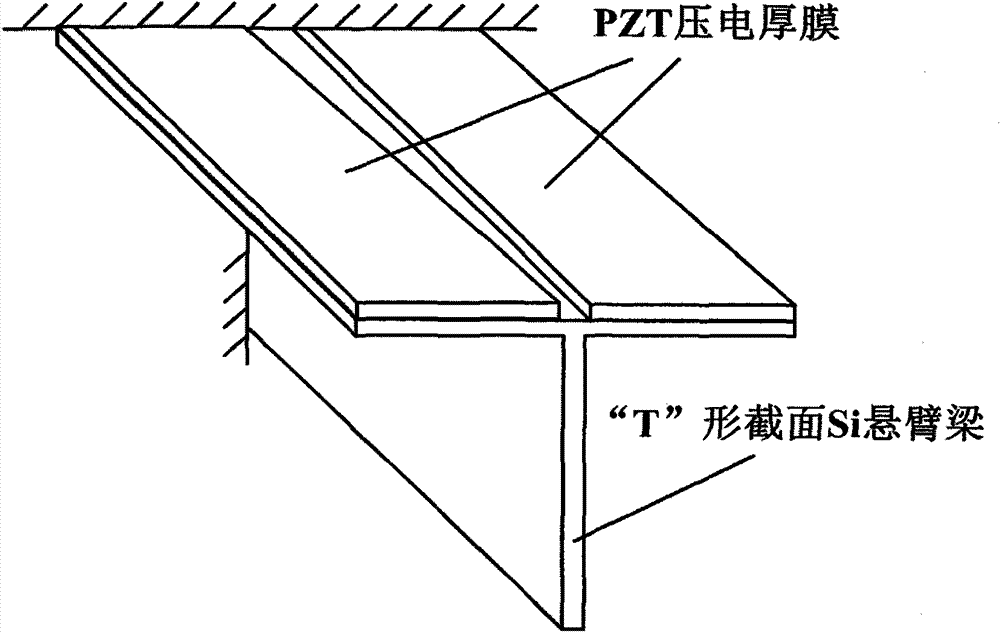
[0028] Such as figure 1 As shown, a transverse MEMS micro-actuator driven by a piezoelectric thick film includes a "T" cross-section cantilever beam formed by a substrate and two PZT piezoelectric thick film driving layers; the two piezoelectric thick film driving layers are located in the " The upper surface of the T”-shaped cross-section cantilever beam is symmetrically distributed, and the thickness of the PZT piezoelectric thick-film driving layer is 2 μm.

[0029] The specific production steps are as follows:

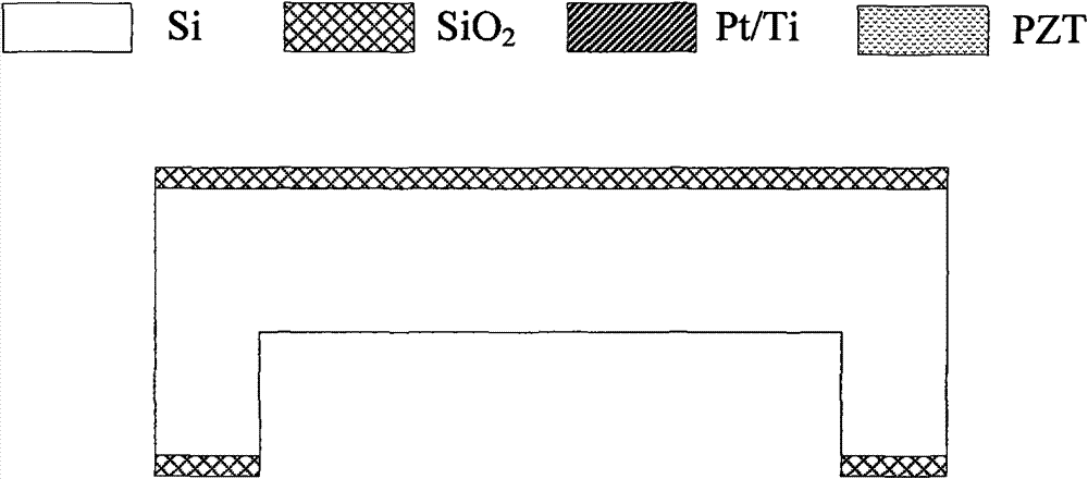
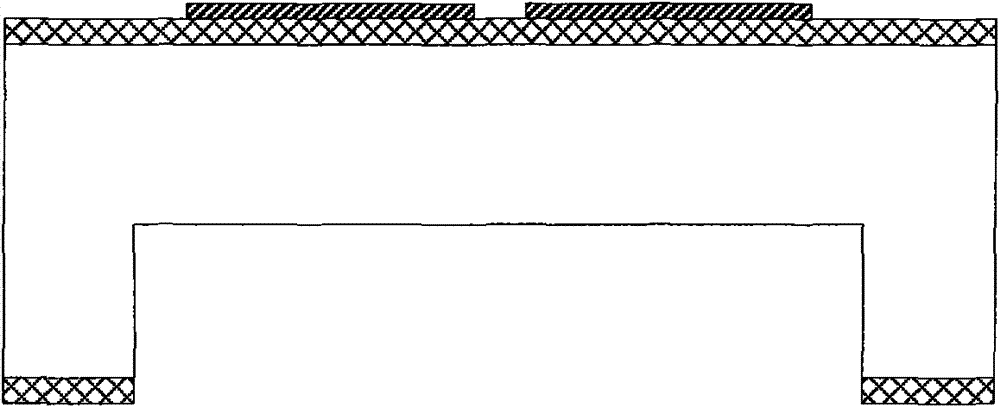
[0030] 1) if figure 2 As shown, first, 2 μm SiO was deposited on both sides of a double-polished (100) Si wafer substrate by a physical enhanced chemical vapor deposition (PECVD) process. 2 barrier layer. After a photolithography process, a photoresist mask pattern is formed on the back of the Si substrate, and SiO is etched by induct...


PUM

PropertyMeasurementUnit
thicknessaaaaaaaaaa
thicknessaaaaaaaaaa
thicknessaaaaaaaaaa

Abstract

The invention relates to a transverse micro electro mechanical system (MEMS) microactuator adopting piezoelectric thick film actuating and a manufacturing method thereof, which belong to the technical field of intelligent materials and structures. The microactuator comprises a cantilever beam and two PZT piezoelectric thick film actuating layers, wherein the cantilever beam is formed by a substrate; the two piezoelectric thick film actuating layers are positioned on the upper surface of the cantilever beam with the T-shaped section, and are distributed symmetrically; and the thickness of the PZT piezoelectric thick film actuating layer is more than 1 mu m. The microactuator provided by the invention has a simple structure, does not comprise an additional motion conversion mechanism, and easily integrates a high-piezoelectric performance PZT thick film; the microactuator is manufactured by adopting a bulk silicon machining process, so low structure freeing difficulties and high manufacturing reliability are ensured; and all manufacturing processes of the piezoelectric transverse MEMS microactuator are compatible with an MEMS process, so the microactuator has the potential of integrated and batch manufacturing, and can be widely applied in the fields of micro-nano operations, micro-nano mechanical movement and walking, electromagnetic signal / micro-nano fluid switching / stop valves, vibrating sensors and the like.

Description

technical field [0001] The invention relates to a transverse MEMS (micro-electro-mechanical system) micro-drive driven by a piezoelectric thick film and a manufacturing method thereof, belonging to the technical field of intelligent materials and structures. Background technique [0002] The movement modes of MEMS micro-actuators can generally be divided into three types: translation, rotation or a combination of the two. For the translation mode, it can be divided into out-of-plane vertical (that is, perpendicular to the direction of the substrate plane) motion and in-plane horizontal (that is, parallel to the direction of the substrate plane) lateral motion. Transverse MEMS micro-driver is a kind of micro-driver that can generate horizontal motion in the plane. Compared with the micro-driver that moves vertically out of the plane, it has the advantages of small in-plane range limitation, strong scalability, and easy monolithic integration. It can be widely used. Used in m...

Claims


Application Information

Patent Timeline
Patent Type & Authority Patents(China)
IPC IPC(8): B81C1/00
Inventor 赵全亮何广平谭晓兰黄昔光袁俊杰曹茂盛
Owner NORTH CHINA UNIVERSITY OF TECHNOLOGY
Learn More