Printed circuit board including embedded passive component and method of fabricating same

a passive component and printed circuit technology, applied in the field of printed circuit boards, can solve the problems of reducing the reliability of electronic goods, short circuit readily occurring between fine circuit patterns,

Inactive Publication Date: 2006-03-16
SAMSUNG ELECTRO MECHANICS CO LTD
View PDF2 Cites 72 Cited by
  • Summary
  • Abstract
  • Description
  • Claims
  • Application Information

AI Technical Summary

Benefits of technology

[0030] Another object of the present invention is to provide a PCB including an embedded passive component, in which a connection between th...

Problems solved by technology

The conventional PCB 200 including the embedded passive components fabricated according to a procedure of FIGS. 2a to 2g is problematic in that since the application of the conductive pastes 215 is implemented using the screen printing process in which there is a large toleranc...

Method used


Image

  • Printed circuit board including embedded passive component and method of fabricating same
  • Printed circuit board including embedded passive component and method of fabricating same
  • Printed circuit board including embedded passive component and method of fabricating same

Examples


first embodiment

[0057] The substrate 1100 having a two-layered structure is described in the first embodiment, but a substrate 1100 having a multi-layered structure, such as a four-, six-, or eight-layered structure, in which predetermined circuit patterns are formed on an internal circuit layer, may be used depending on the purpose and application.

[0058] As shown in FIG. 3b, after two via holes (A1) are formed to achieve circuit connection between the upper and lower copper foil layers 1120, 1120′ of the substrate 1100, copper plating layers 1130, 1130′ are formed on the upper and lower copper foil layers 1120, 1120′ and on walls of the via holes (A1) so as to electrically connect the via holes (A1) to each other.

[0059] At this time, since each of the via holes (A1) formed through the substrate 1100 is a through hole connecting the copper foil layers 1120, 1120′ to each other, it is preferable to form the via holes (A1) at predetermined positions using a mechanical drill such as a computer numeri...

second embodiment

[0103]FIGS. 6a to 6j are sectional and top views illustrating the fabrication of a PCB including an embedded passive component according to the present invention.

[0104] As shown in FIG. 6a, a copper clad laminate as a substrate 2100 is provided, in which copper foil layers 2120, 2120′ are applied on an insulating resin layer 2110.

[0105] In this case, only a two-layered substrate 2100 is employed. However, a substrate 2100 having a multi-layered structure, such as four-, six-, or eight-layered structures, may be used depending on the purpose and application.

[0106] As shown in FIG. 6b, after two via holes (B1) are formed to achieve circuit connection between the upper and lower copper foil layers 2120, 2120′ of the substrate 2100, copper plating layers 2330, 2330′ are formed on the upper and lower copper foil layers 2120, 2120′ and on walls of the via holes (B1) so as to electrically connect the via holes (B1) to each other.

[0107] It is preferable to form the via holes (B1) through...

third embodiment

[0153] Subsequently, a traditional PCB build-up process is conducted, thereby creating the PCB including the embedded passive component according to the present invention.

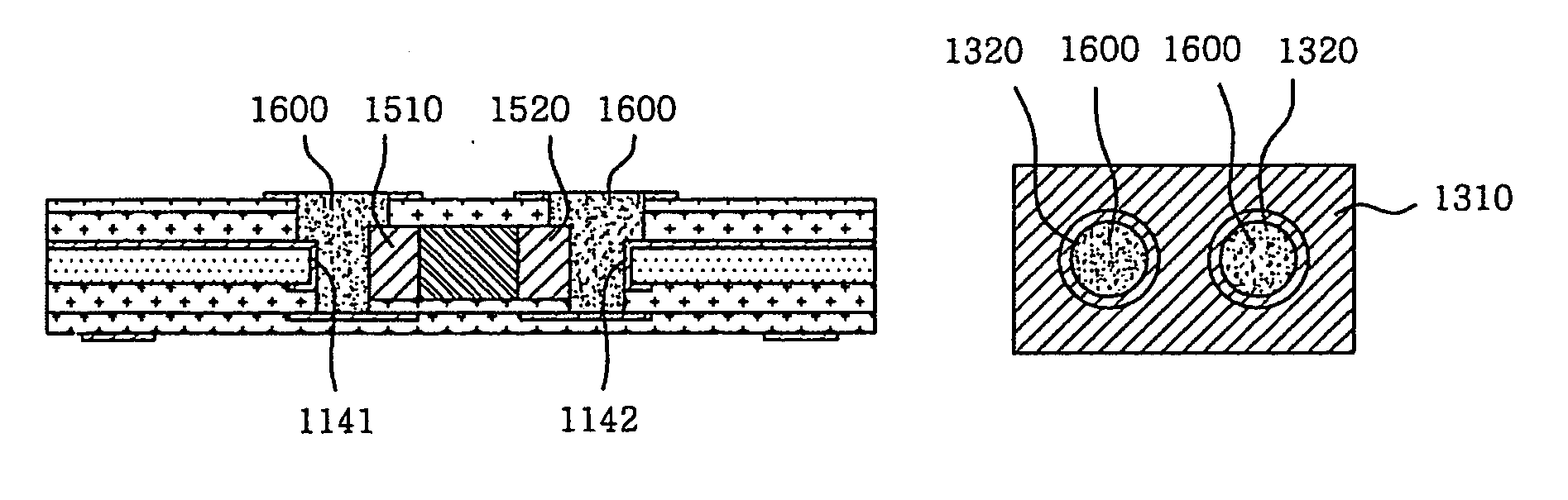
[0154] After the step of FIG. 9f, as shown in FIG. 9h, a copper plating layer 3300 may be formed between the terminals 3141, 3142 and electrodes 3510, 3520 of the passive component so as to electrically connect the terminals 3141, 3142 to the electrodes 3510, 3520 of the passive component.

[0155] Next, a traditional PCB build-up process is conducted, thereby creating the PCB including the embedded passive component according to an embodiment of the present invention.

[0156]FIGS. 10a and 10b are perspective views of embedded passive components according to further embodiments of the present invention.

[0157] As shown in FIG. 10a, the embedded passive component 4500 according to an embodiment of the present invention is embedded in an insulating layer of a PCB including the embedded passive component, and has electro...


PUM

PropertyMeasurementUnit
Electrical conductoraaaaaaaaaa
Distanceaaaaaaaaaa
aaaaaaaaaa

Abstract

Disclosed is a PCB including an embedded passive component and a method of fabricating the same. The PCB includes at least two circuit layers in which circuit patterns are formed. At least one insulating layer is interposed between the circuit layers. A pair of terminals is vertically formed through the insulating layers, plated with a first conductive material, and separated from each other by a predetermined distance. The embedded passive component is interposed between the terminals and has electrodes formed on both sides thereof. The electrodes are separated from the terminals by a predetermined distance and electrically connected to the terminals through a second conductive material.

Description

INCORPORATION BY REFERENCE [0001] The present application claims priority under 35 U.S.C. §119 to Korean Patent Application No. 2004-73822 filed on Sep. 15, 2004. The content of the application is incorporated herein by reference in its entirety. BACKGROUND OF THE INVENTION [0002] 1. Field of the Invention [0003] The present invention relates, in general, to a printed circuit board (PCB) including an embedded passive component and a method of fabricating the same and, more particularly, to a PCB including an embedded passive component, in which the passive component is mounted in a predetermined receiving hole for communicating with via holes, and in which walls of the via holes are used as terminals connected to electrodes of the passive component, and a method of fabricating the same. [0004] 2. Description of the Prior Art [0005] Recently, electronic technologies are moving toward the embedding of resistors, capacitors, integrated circuits (IC) or the like into a substrate so as t...

Claims


Application Information

Patent Timeline
IPC IPC(8): H05K7/06
CPCH05K1/185H05K3/4069H05K3/4602H05K2201/09536H05K2201/10636Y10T29/49165Y10T29/49101Y10T29/49124Y10T29/49155Y10T29/49126H05K2203/063Y02P70/50H05K1/18H05K3/46
Inventor RYU, CHANG SUPKANG, MYUNG SAM
Owner SAMSUNG ELECTRO MECHANICS CO LTD
Why Eureka
Try Eureka