

Method and system for calibrating a laser processing system and laser marking system utilizing same
a laser processing system and laser marking technology, applied in the field of method and system for calibrating a laser processing system and laser marking system utilizing same, can solve problems such as poor mark quality or mark positioning errors
- Summary
- Abstract
- Description
- Claims
- Application Information
AI Technical Summary
Benefits of technology
Problems solved by technology
Method used
Image

Examples
Embodiment Construction
Overview
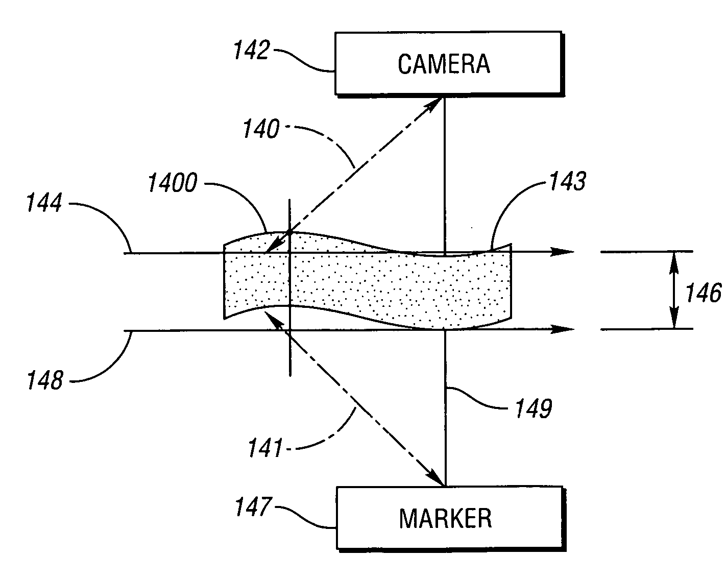
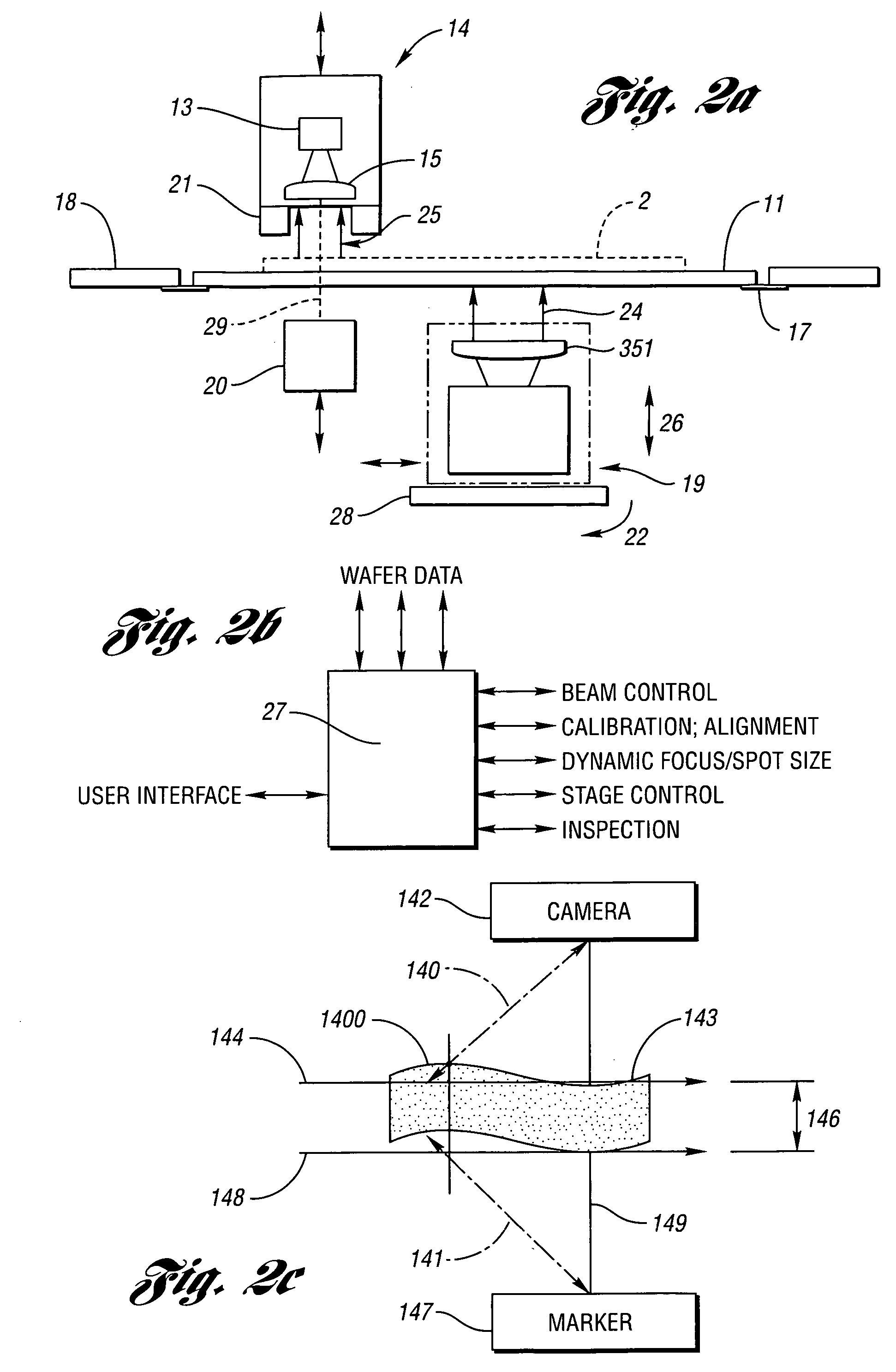
[0060] Several components of a system 100 for laser marking and inspection of wafers, for instance 300 mm wafers, is schematically illustrated in FIG. 5A. A robot 101 transfers a wafer from a FOUP (Front Opening Unified Portal) delivery device to a pre-aligner 102 which is used to find the notch or flat of the wafer so as to orient the wafer for further processing. Reader 103 may be used to extract certain coded information which in turn may be used in subsequent processing steps. A precision stage 104 is used, and a fine alignment procedure included to correct the residual error of the pre-aligner (e.g., X, Y, rotation). The wafer is marked. All marks, or a designated subset, are then inspected. In the arrangement of FIG. 5A the inspection system is used with a separate inspection stage 105.
[0061] A marking sequence, following opening of a FOUP, includes: [0062] 1. Robot moves the wafer to the pre-aligner and establishes a notch-die positional relation. [0063] 2. The waf...
PUM
| Property | Measurement | Unit |
|---|---|---|
| thickness | aaaaa | aaaaa |
| thickness | aaaaa | aaaaa |
| diameter | aaaaa | aaaaa |
Abstract
Description
Claims
Application Information