Light emitting diode improved in luminous efficiency

a technology of light-emitting diodes and luminous efficiency, which is applied in the direction of basic electric elements, electrical equipment, and semiconductor devices, can solve the problems of light loss and lower and achieve the effect of improving the luminous efficiency of leds and high reflectivity material layers

Inactive Publication Date: 2006-03-16
SAMSUNG ELECTRO MECHANICS CO LTD
View PDF5 Cites 38 Cited by
  • Summary
  • Abstract
  • Description
  • Claims
  • Application Information

AI Technical Summary

Benefits of technology

[0015] The present invention has been made to solve the foregoing problems of the prior art and it is therefore an object of the present invention to provide a high reflectivity material layer between an n-electrode and a partial region of an underlying n-doped semiconductor layer in order to reflect light toward a substrate thereby improving the luminous efficiency of an LED.

Problems solved by technology

This as a result causes light loss and therefore lowers the luminous efficiency of the LED 100.

Method used


Image

  • Light emitting diode improved in luminous efficiency
  • Light emitting diode improved in luminous efficiency
  • Light emitting diode improved in luminous efficiency

Examples


first embodiment

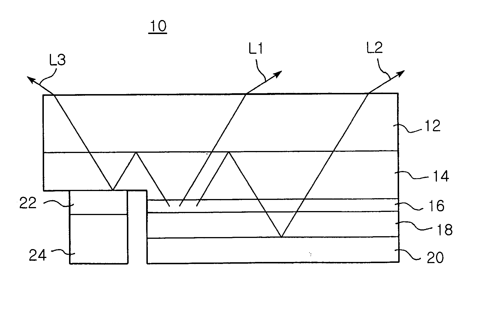
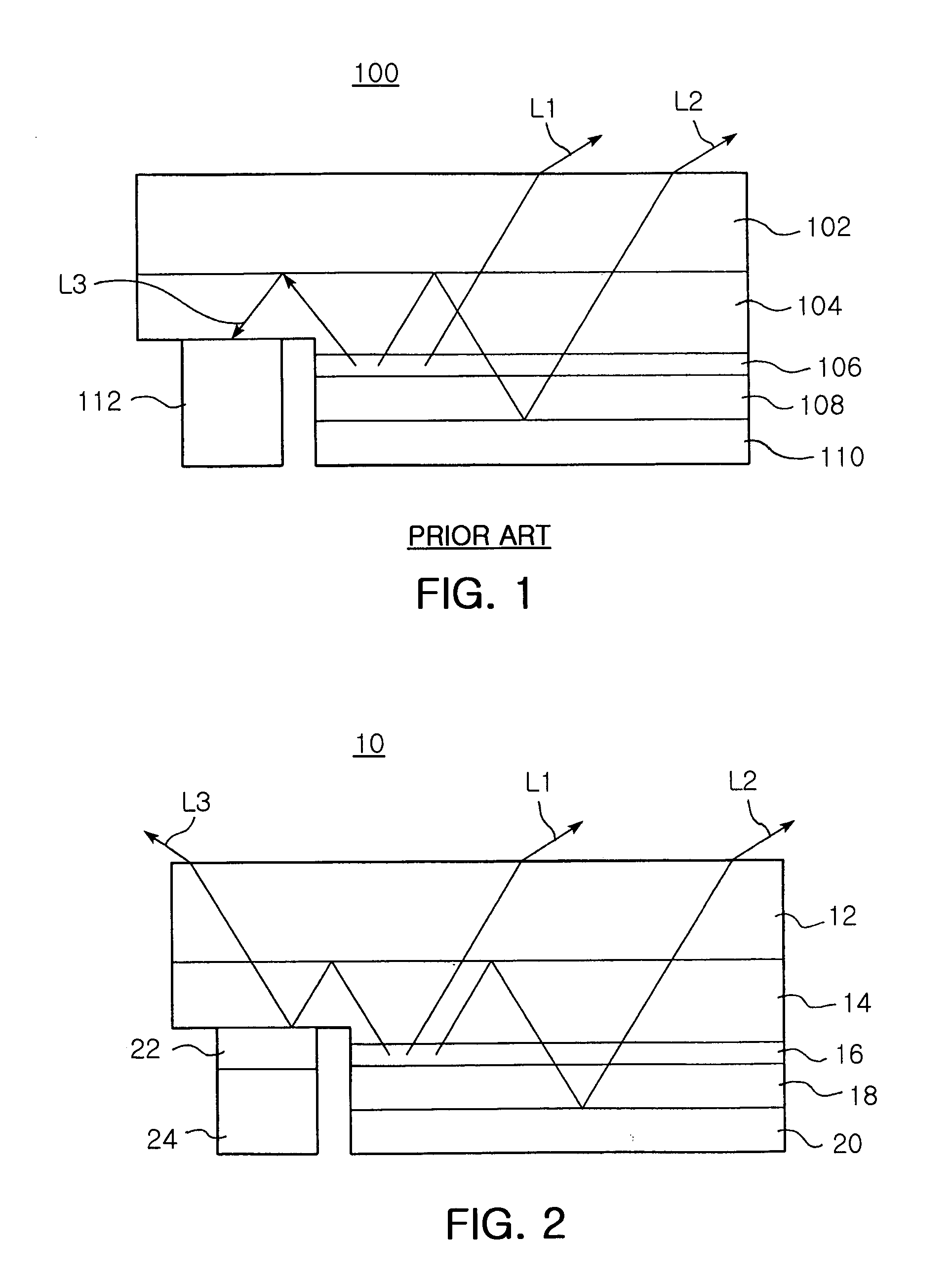
[0038]FIG. 2 is a cross-sectional view of an LED according to the invention, which illustrates light reflected from an n-electrode.

[0039] As shown in FIG. 2, an LED 10 of the invention has an improved luminous efficiency, and includes a substrate 12 of for example sapphire (Al2O3), an n-doped semiconductor layer 14 of for example n-GaN grown on the sapphire substrate 12, an active layer 16 grown on a first region occupying a major portion of the n-doped semiconductor layer 14 and a p-doped semiconductor layer 18 of for example-p-GaN grown on the active layer 16. The n-doped semiconductor layer 14, the active layer 16 and the p-doped semiconductor layer 18 are epitaxially grown via Metal Organic Chemical Vapor Deposition (MOCVD), and then etched into a mesa structure to expose a second region of the n-doped semiconductor layer 14 except for the first region.

[0040] The LED 10 improved in luminous efficiency includes a p-electrode 20 formed on the p-doped semiconductor layer 18. The p...

second embodiment

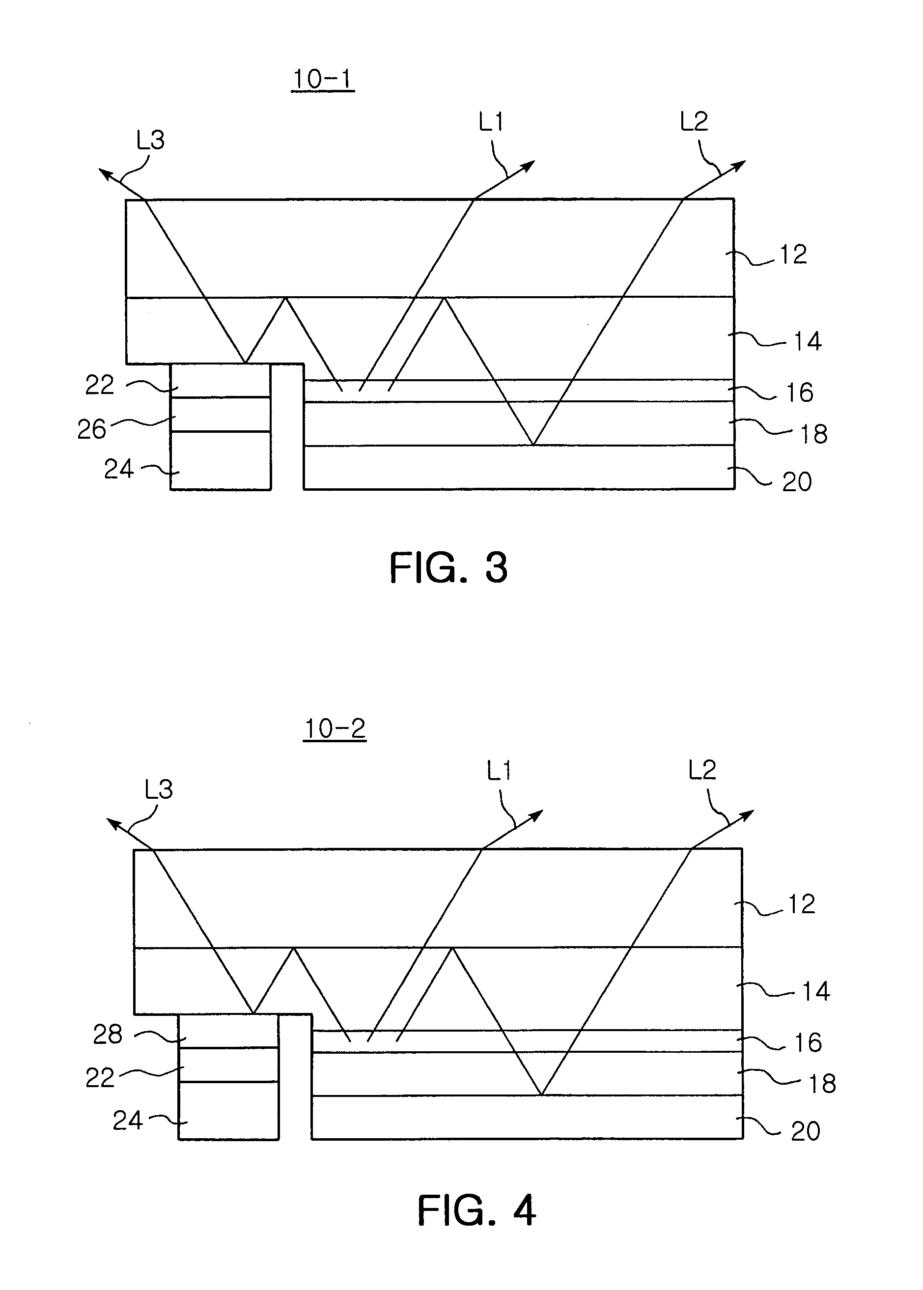
[0056]FIG. 3 is a cross-sectional view of an LED according to the invention, which illustrates light reflected from an n-electrode.

[0057] Referring to FIG. 3, an LED 10-1 according to the second embodiment of the invention has a structure substantially similar to that of the LED 10 of the first embodiment shown in FIG. 2. That is, the LED 10-1 includes an n-doped semiconductor layer 14 (e.g., of n-GaN), an active layer 16, a p-doped semiconductor layer 18 (e.g., p-GaN) and a p-electrode 20, which are formed in their order on the substrate 12 into a mesa structure. Structures and forming techniques of these components are substantially the same as those of the first embodiment as described above.

[0058] In addition, a high reflectivity material layer 22, an intermediate layer 26 and an n-electrode 24 are formed on a partial first region of the n-doped semiconductor layer 14. The high reflectivity material layer 22 and the n-electrode 24 will not be described further since they are su...

third embodiment

[0064]FIG. 4 is a cross-sectional view of an LED according to the invention, which illustrates light reflected from an n-electrode.

[0065] Referring to FIG. 4, the LED 10-2 according to the third embodiment of the invention has a structure substantially similar to that of the LED 10 of the first embodiment shown in FIG. 2. That is, the LED 10-2 includes an n-doped semiconductor layer 14 (e.g., of n-GaN), an active layer 16, a p-doped semiconductor layer 18 (e.g., p-GaN) and a p-electrode 20, which are formed in their order on a sapphire substrate 12 into a mesa structure. Structures and forming techniques of these components are substantially the same as those of the first embodiment as described above.

[0066] In addition, a conductive oxide layer 28, a high reflectivity material layer 22 and an n-electrode 24 are formed on a partial second region of the n-doped semiconductor layer 14. The high reflectivity material layer 22 and the n-electrode 24 will not be described further since ...


PUM


Abstract

The present invention relates to an LED, in which an n-doped semiconductor layer, an active layer, a p-doped semiconductor layer and a p-electrode are formed in their order on a sapphire substrate. A high reflectivity material layer containing Cu and Si is deposited on a remaining partial region of the n-doped semiconductor layer. An n-electrode is formed on the high reflectivity material layer. The high reflectivity material layer formed between the n-electrode and the partial region of the underlying n-doped semiconductor layer can reflect light toward a substrate, thereby improving the luminous efficiency of the LED.

Description

RELATED APPLICATION [0001] The present application is based on, and claims priority from, Korean Application Number 2004-73194, filed Sep. 13, 2004, the disclosure of which is hereby incorporated by reference herein in its entirety. BACKGROUND OF THE INVENTION [0002] 1. Field of the Invention [0003] The present invention relates to a Light Emitting Diode (LED), more particularly, which has a high reflectivity material layer formed between an n-electrode and a partial region of an underlying n-doped semiconductor layer in order to reflect light toward a substrate, thereby improving the luminous efficiency of the LED. [0004] 2. Description of the Related Art [0005] In general, LEDs for obtaining blue or green lights are fabricated using nitride-based semiconductors such as InAlGaN. [0006] Currently, demand for flip chip types among various LED types is increasing. In case of a flip chip type LED, light generated from an active layer is radiated to the outside directly through a sapphi...

Claims


Application Information

Patent Timeline
Patent Type & Authority Applications(United States)
IPC IPC(8): H01L33/00H01L33/10H01L33/32H01L33/40H01L33/62
CPCH01L33/405H01L33/32
Inventor SHIN, HYOUN SOOYI, BONG IIRO, JAE CHULPYEON, IN JOON
Owner SAMSUNG ELECTRO MECHANICS CO LTD
Why Eureka
Try Eureka