AI technical title is built by Patsnap AI team. It summarizes the technical point description of the patent document.
a technology of semiconductors and modules, applied in the direction of voltage-current phase angles, basic electric elements, instruments, etc., can solve problems such as voltage drop
Inactive Publication Date: 2006-03-16
KK TOSHIBA
View PDF6 Cites 73 Cited by
Summary
Abstract
Description
Claims
Application Information
AI Technical Summary
This helps you quickly interpret patents by identifying the three key elements:
Problems solved by technology
Method used
Benefits of technology
Problems solved by technology
In a form of supplying power from a single power source to a plurality of circuits, even slight parasitic impedance on a wire causes a voltage drop.
Accordingly, a voltage required for the circuit is not supplied, which causes erroneous operations.
Method used
Image
Click on the blue label to locate the original text in one second.
Reading with bidirectional positioning of images and text.
Examples
first embodiment
(Modification of First Embodiment)
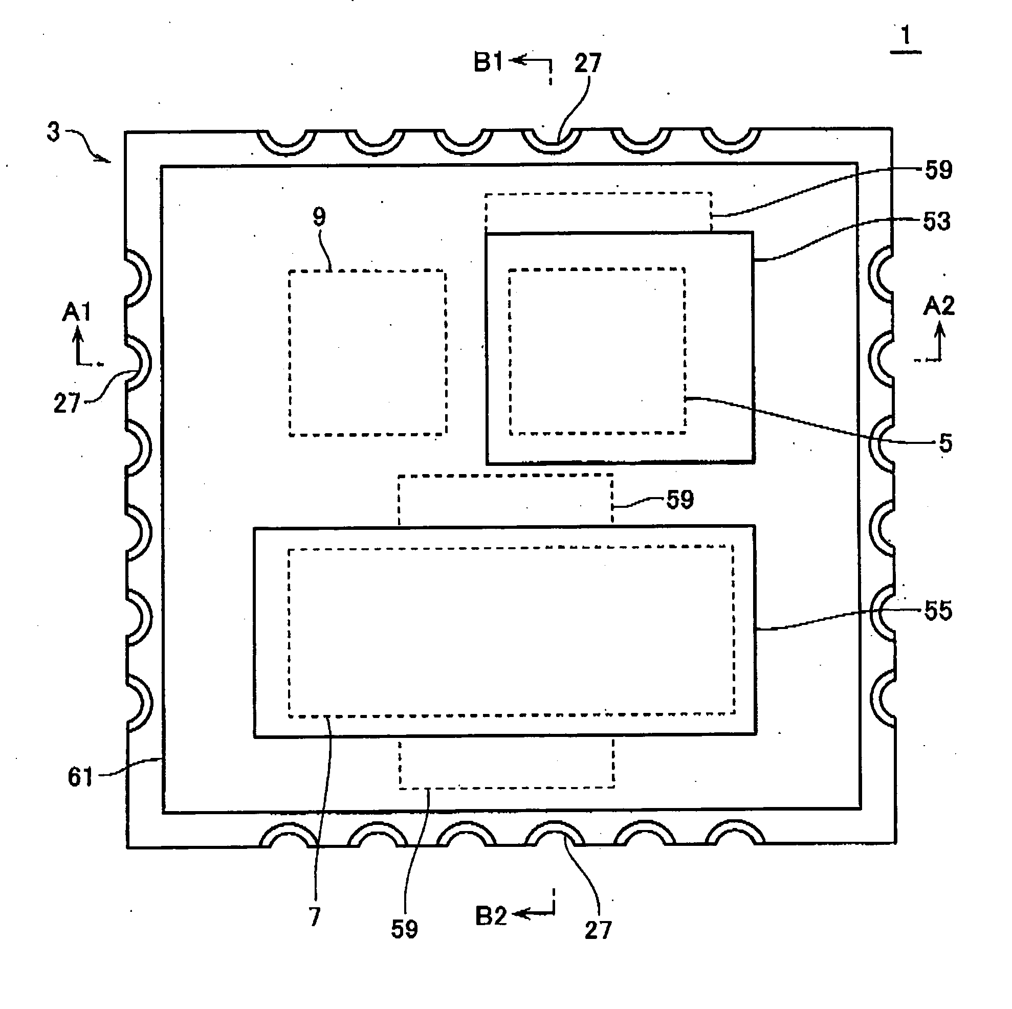
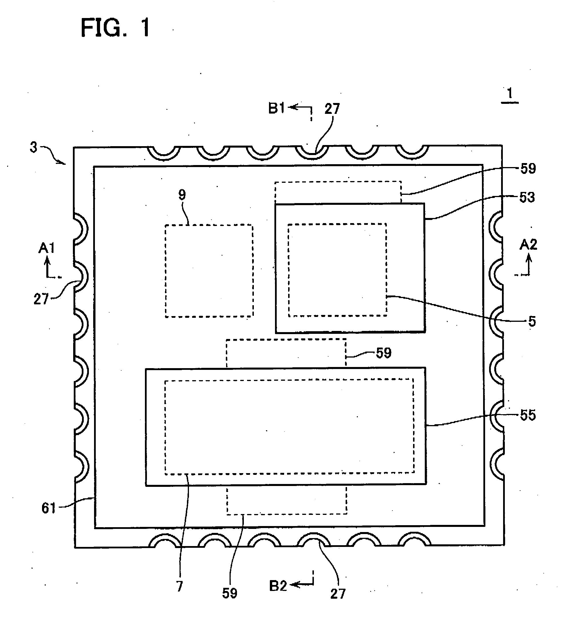
[0105]FIG. 7 is a plan view of a modification of the semiconductor module 1 according to the first embodiment, corresponding to FIG. 1. The power MOS chip 7 configures a low-potential circuit while the power MOS chip 5 configures a high-potential circuit. The power MOS chip 7 is split into three chips 7-1, 7-2, 7-3. At this point, the semiconductor module 1 in FIG. 7 differs from that in FIG. 1. The heat sink member 55 has regions corresponding to the chips 7-1, 7-2, 7-3, which serve as heat sink members for the respective chips. Therefore, it can be said in this case that a plurality of heat sink members are linked with each other to configure a single heat sink plate (heat sink member 55).
[0106] The power MOS chip 7 in FIG. 1 has relatively large dimensions with a large thermal expansion efficiency and a large thermal stress. In the modification of FIG. 7, the power MOS chip 7 is split into three relatively small chips 7-1, 7-2, 7-3 to ensure the...
second embodiment
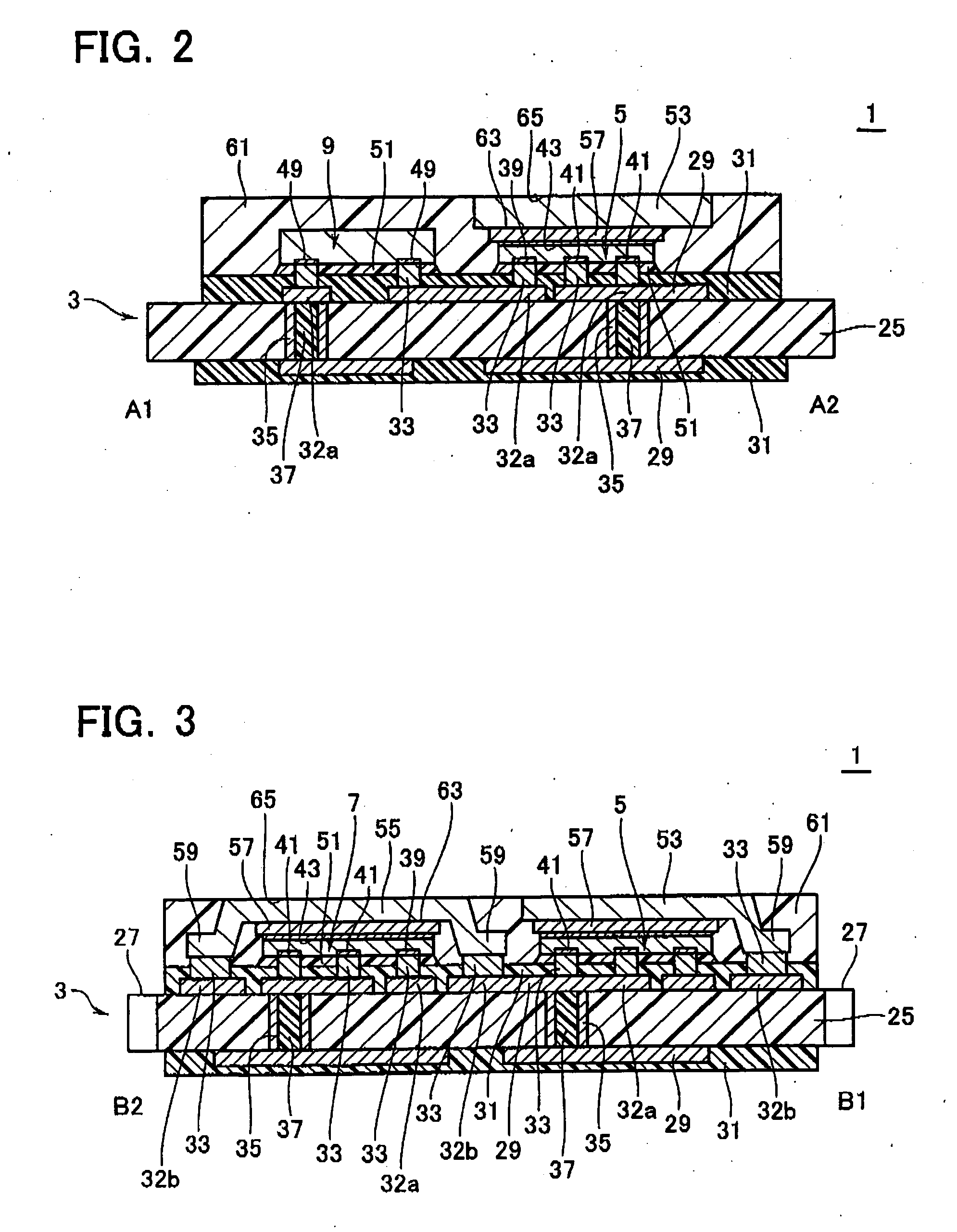
[0108]FIG. 8 is a plan view of a semiconductor module 1 according to a second embodiment. FIG. 9 is a cross-sectional view taken along C1-C2 line in FIG. 8. FIGS. 8 and 9 are employed to describe the second embodiment about differences from the first embodiment.
[0109] In the second embodiment, the heat sink member 53 covering the power MOS chip 5 extends over the drive IC chip 9 so as to cover the drive IC chip 9. The power MOS chip 5 and the drive IC chip 9 share the heat sink member 53. A separate heat sink member for covering the drive IC chip 9 may be arranged aside from the heat sink member 53. In comparison with such the case, the heat sink member can be given a larger area, which improves the heat radiation by the extent.
[0110] The drive IC chip 9 has a lower surface 77 kept at the ground potential, which differs from the potential on the drain electrode 43 of the power MOS chip 5. Therefore, the heat sink member 53 is insulated from the drive IC chip 9 via a resinous membe...
third embodiment
[0116] Different from the preceding embodiment, a third embodiment comprises a low-potential power MOS chip with a built-in SBD. FIG. 12 is a cross-sectional view of part of the low-potential power MOS chip 7a provided in the third embodiment, corresponding to the power MOS chip 7 in FIG. 4. An SBD 69 is formed at a certain distance away from an end terminal 81 of a MOSFET formation region. The certain distance means a distance that prevents the MOSFET and the SBD from interfering with each other.
[0117] The SBD 69 includes an epitaxial layer 11 and a metal layer 83 such as aluminum formed thereon. When the epitaxial layer 11 makes contact with the metal layer 83, a Schottky barrier is made at the contact portion. The SBD 69 is connected in parallel with the MOSFET in the power MOS chip 7. A p-n junction diode may be employed instead of the SBD 69.
[0118] When the power MOS chip 7a with the built-in SED 69 is employed in the semiconductor module as in the third embodiment, the numbe...
PUM
Abstract
A semiconductor module comprises a mounting board. A plurality of power switching device chips are mounted on the mounting board by flip-chip bonding. The chip has an upper surface and a lower surface and is configured to face the upper surface toward the mounting board. A drive IC chip is mounted on the mounting board by flip-chip bonding. The drive IC chip is operative to drive gates of transistors formed in the plurality of power switching device chips. A plurality of heat sink members are located on the lower surfaces of the plurality of power switching device chips, respectively. A resinous member is provided to seal the plurality of power switching device chips and the drive IC chip in a single package.
Description
CROSS-REFERENCE TO RELATED APPLICATION [0001] This application is based on and claims the benefit of priority from prior Japanese Patent Application No. 2004-253276, filed on Aug. 31, 2004, the entire contents of which are incorporated herein by reference. BACKGROUND OF THE INVENTION [0002] 1. Field of the Invention [0003] The present invention relates to a semiconductor module such as a multi-chip module. [0004] 2. Description of the Related Art [0005] A DC-DC converter is a device that converts a certain voltageDC current into a different voltageDC current. The DC-DC converter is highly efficient and can be downsized. Therefore, it has been utilized as a power source incorporated in small electronic instruments (for example, information communications instruments such as notebook personal computers and mobile phones). [0006] In the information communications instruments such as PCs, a CPU is fine patterned and sped up to provide an advanced low-voltage / large-current power source...
Claims
Application Information
Patent Timeline
Application Date:The date an application was filed.
Publication Date:The date a patent or application was officially published.
First Publication Date:The earliest publication date of a patent with the same application number.
Issue Date:Publication date of the patent grant document.
PCT Entry Date:The Entry date of PCT National Phase.
Estimated Expiry Date:The statutory expiry date of a patent right according to the Patent Law, and it is the longest term of protection that the patent right can achieve without the termination of the patent right due to other reasons(Term extension factor has been taken into account ).
Invalid Date:Actual expiry date is based on effective date or publication date of legal transaction data of invalid patent.

