Semiconductor device

a semiconductor device and device technology, applied in the direction of semiconductor/solid-state device testing/measurement, semiconductor device details, semiconductor/solid-state device testing/measurement, etc., can solve the problem of inability to reduce the contour size of the sip down to a contour size, the defect analysis of the sdram cannot be performed, and the detailed evaluation, reliability test, and reliability analysis cannot be performed. to achieve the effect of reducing the contour size of the semiconductor devi

Active Publication Date: 2006-03-23
RENESAS ELECTRONICS CORP
View PDF4 Cites 35 Cited by
  • Summary
  • Abstract
  • Description
  • Claims
  • Application Information

AI Technical Summary

Benefits of technology

[0010] It is an object of the present invention to provide a technique of reducing the contour size of a semiconductor device including a first semiconductor chip having a memory circuit and a second semiconductor chip having a circuit controlling the memory circuit down to a size required by a client without impairing the testability of the first semiconductor chip having the memory circuit.

Problems solved by technology

Under these circumstances, it has been become more difficult to secure an area on which the external terminals are disposed.
This makes it impossible to reduce the contour size of an SiP down to a contour size required by a client.
If the testing external terminals are simply omitted, there arises the problem that detailed evaluation, reliability test, and defect analysis of the SDRAM cannot be performed.

Method used


Image

  • Semiconductor device
  • Semiconductor device
  • Semiconductor device

Examples


embodiment 1

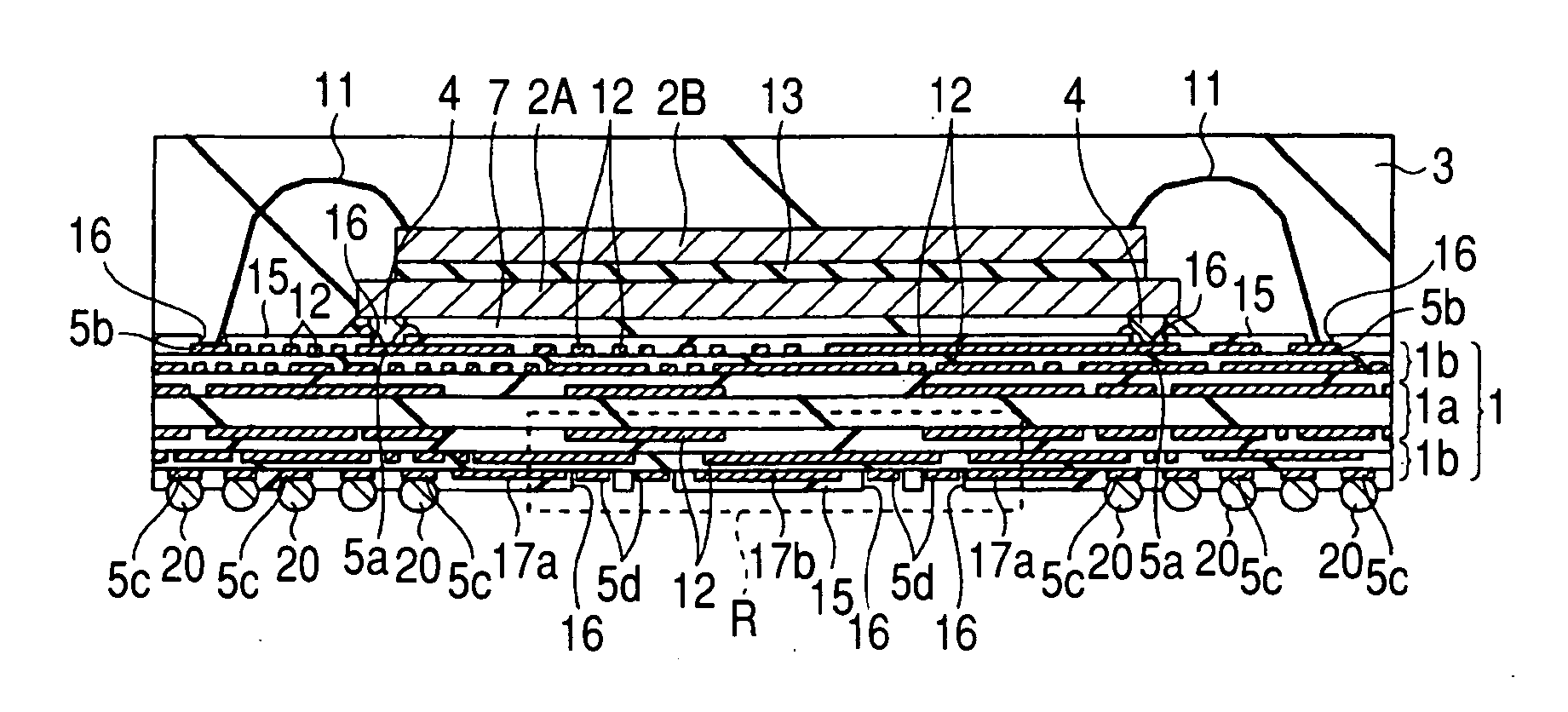
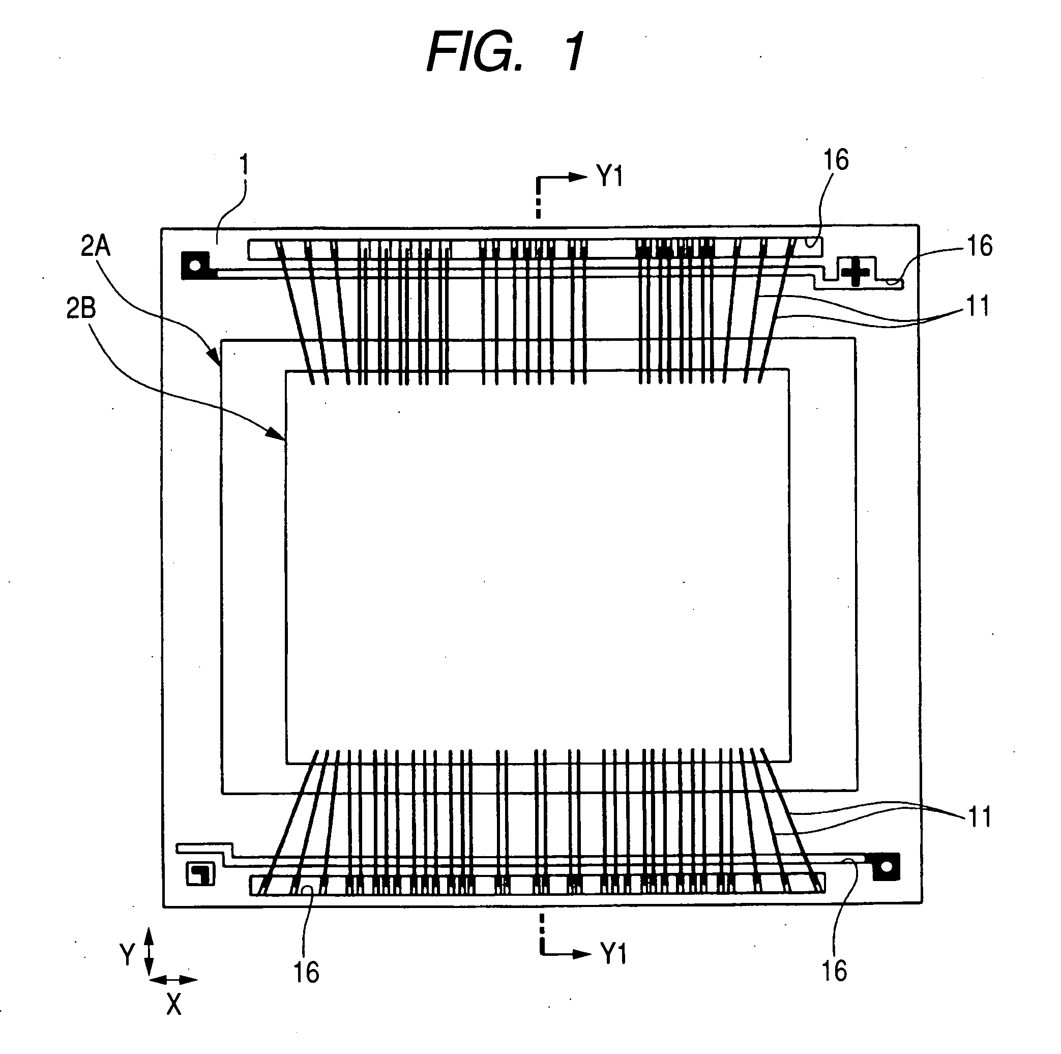
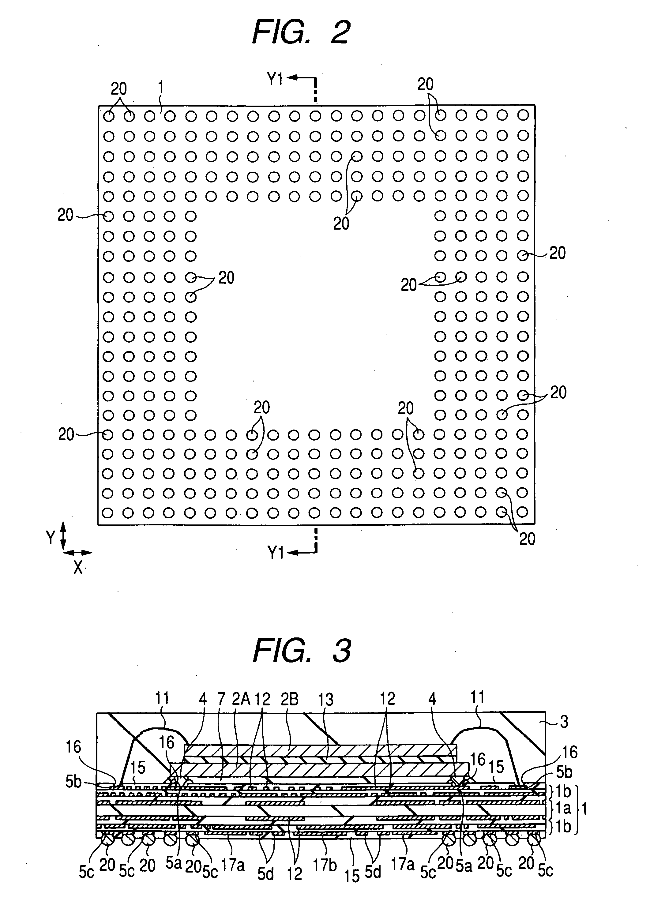
[0039]FIG. 1 is a plan view of the top plane (first main surface) of an interconnect substrate showing the internal structure of a semiconductor device of the present embodiment. FIG. 2 is a plan view of the bottom plane (second main surface) of the interconnect device of the semiconductor device shown in FIG. 1. FIG. 3 is a cross-sectional view taken on line Y1-Y1 of FIGS. 1 and 2. FIG. 4 is a plan view of a main surface of a second semiconductor chip of the semiconductor device shown in FIG. 1. FIG. 5 is a plan view of a main plane of a first semiconductor chip of the semiconductor device shown in FIG. 1. FIG. 6 is a table illustrating numbers given to the terminals of the first semiconductor chip shown in FIG. 5, as well as the names of the terminals. FIG. 7 is a plan view of the lowermost interconnect layer (second main surface) of the interconnect substrate of the semiconductor device shown in FIG. 1. FIG. 8 is a fragmentary plan view of the top-level interconnect layer (first ...

embodiment 2

[0063]FIG. 19 is a plan view of the bottom surface of a semiconductor device of the present Embodiment 2. FIG. 20 is a cross-sectional view taken on line Y2-Y2 of FIG. 19. FIG. 21 is an enlarged cross section of an area R of FIG. 20. FIG. 22 is a cross-sectional view of a modification of the device shown in FIG. 21.

[0064] In the present Embodiment 2, the surfaces of the electrodes 5d on the bottom surface of the interconnect substrate 1 of the semiconductor device are exposed from the solder resist 15. Openings 16 in which the electrodes 5d are exposed are formed simultaneously with when openings 16 in which the electrodes 5c are exposed are formed.

[0065] One method of exposing the electrodes 5d is to place the opening ends of the solder resist 15 remotely from the outer peripheries of the electrodes 5d such that the opening ends do not reach the outer peripheries (non solder mask defined (NSMD)) as shown in FIG. 21. Alternatively, the opening ends of the solder resist 15 may reac...


PUM


Abstract

There is disclosed a semiconductor device having first and second semiconductor chips. The first semiconductor chip has a memory circuit. The second semiconductor chip has a circuit controlling the memory circuit. The contour size of the semiconductor device is reduced down to a smaller size required by a client without impairing the testability of the first semiconductor chip having the memory circuit. The circuit controlling the memory circuit consists of an MPU. The memory circuit consists of an SDRAM. The two semiconductor chips are stacked on top of each other over the top surface of an interconnect substrate. The chips are sealed in a molding resin, thus forming an SiP (System-in-Package). First terminals electrically connected with the second chip are arranged as external terminals of the SiP on the outer periphery of the bottom surface of the interconnect substrate. Plural second electrodes electrically connected with interconnects, which electrically connect the two chips, are mounted as terminals for testing of the SDRAM. The second electrodes are located more inwardly than the innermost row of the first external electrodes on the bottom surface of the interconnect substrate.

Description

CROSS-REFERENCE TO RELATED APPLICATION [0001] The present invention claims priority from Japanese patent application No. 2004-273024, filed on Sep. 21, 2004, the content of which is hereby incorporated by reference into this application. BACKGROUND OF THE INVENTION [0002] 1. Field of the Invention [0003] The present invention relates to semiconductor device technology and, more particularly, to a technique that is effectively applied to a semiconductor device in the form of a System-in-Package (SiP) comprising a desired circuit system built within a package. The circuit system uses a semiconductor chip having a memory circuit and another semiconductor chip having a circuit that controls the memory circuit. [0004] 2. Description of the Related Art [0005] We have discussed a System-in-Package (SiP) comprising a package in which both a semiconductor chip having a microcomputer and another semiconductor chip having a synchronous DRAM (synchronous dynamic random access memory; abbreviate...

Claims


Application Information

Patent Timeline
Patent Type & Authority Applications(United States)
IPC IPC(8): H01L23/48H01L23/52
CPCH01L22/32H01L23/49816H01L23/49838H01L24/45H01L24/49H01L25/0657H01L25/18H01L2224/45144H01L2224/48091H01L2224/48227H01L2224/49171H01L2224/49175H01L2225/0651H01L2225/06517H01L2225/06582H01L2225/06596H01L2924/01002H01L2924/01004H01L2924/01005H01L2924/01013H01L2924/01028H01L2924/01029H01L2924/01047H01L2924/0105H01L2924/01078H01L2924/01079H01L2924/01082H01L2924/14H01L2924/15311H01L2924/19041H01L24/48H01L2924/01006H01L2924/01023H01L2924/01033H01L2924/014H01L2924/12041H01L2224/16225H01L2224/32145H01L2224/32225H01L2224/73204H01L2224/73265H01L2224/0401H01L2224/06179H01L2224/05553H01L2224/0603H01L2924/00014H01L2924/00H01L2924/00012H01L2924/181H01L24/73H01L2924/10161H01L2224/73253
Inventor HAYASHI, YOSHINARIISHIKAWA, TOSHIKAZUHOSHINO, TAKAYUKI
Owner RENESAS ELECTRONICS CORP
Why Eureka
Try Eureka