Method for producing electron beam apparatus
a technology of electron beam and apparatus, which is applied in the manufacture of sparking plugs, lighting and heating apparatuses, and tube/lamp factory adjustment, etc., can solve the problems of deterioration of components, electric emission, and becoming a very annoying obstacl
- Summary
- Abstract
- Description
- Claims
- Application Information
AI Technical Summary
Benefits of technology
Problems solved by technology
Method used
Image

Examples
example 1
[0098] This example is to execute an SE detection before sealing, and to execute an SE elimination by a local conditioning.
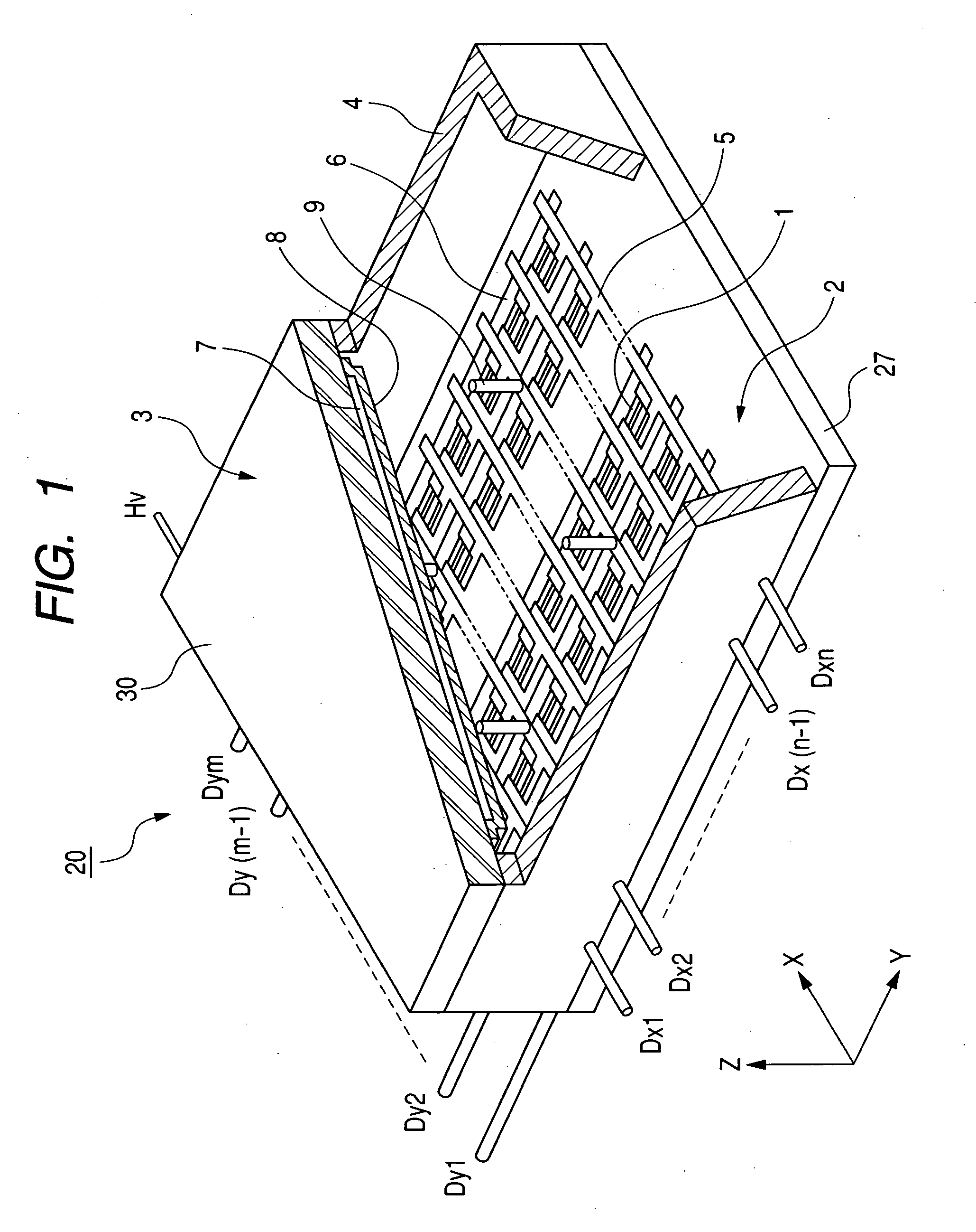
[0099] (Outline of Display Panel)
[0100] A display panel 20 of the image display apparatus to be produced is as already explained in FIG. 1, and maintains a vacuum of about 10−5 Pa therein.
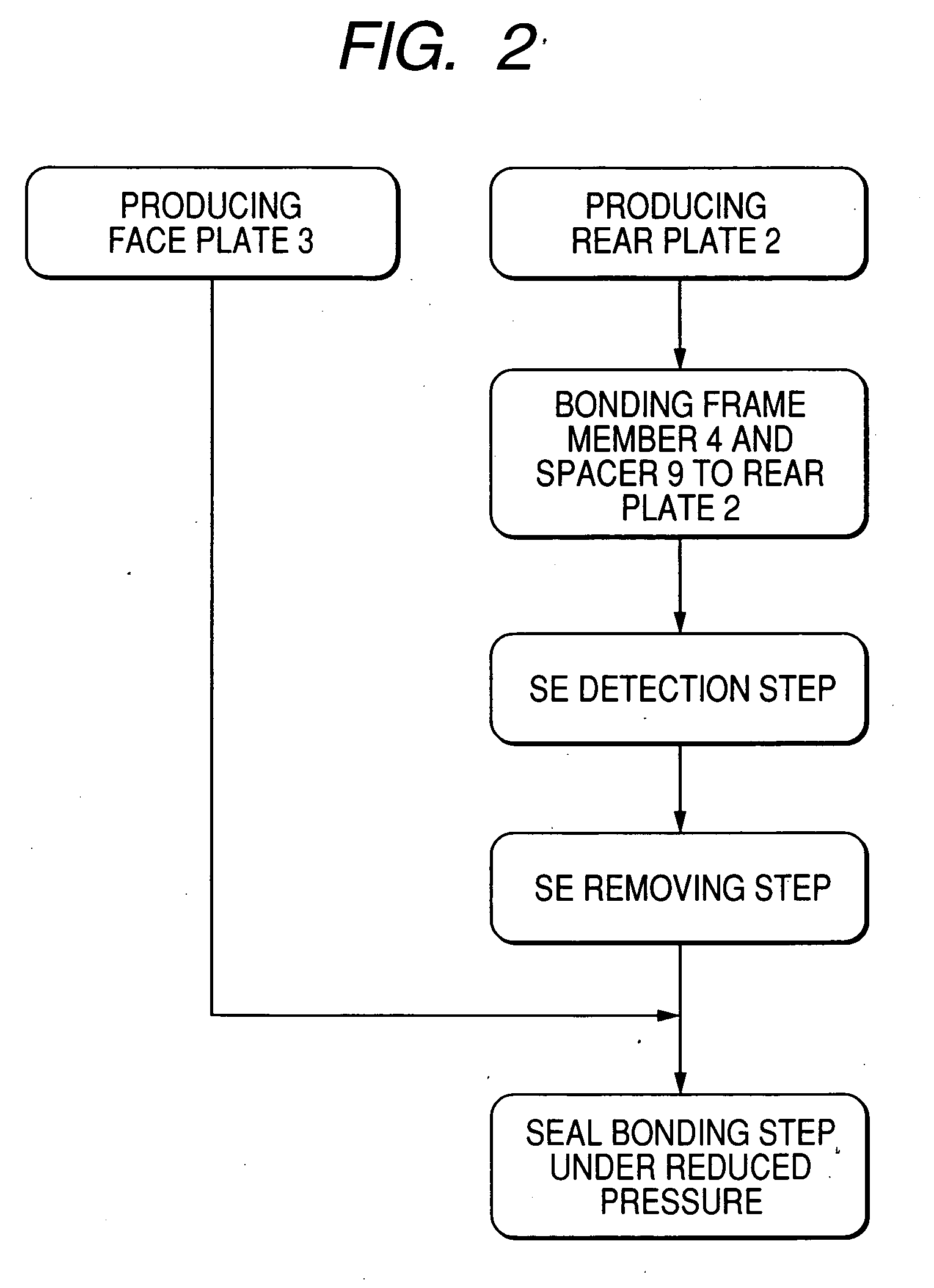
[0101] (Preparation of Rear Plate)
[0102] As shown in FIG. 1, the rear plate 2 is provided with plural electron-emitting devices 1. Such electron-emitting devices 1 are cold cathode devices, and are representatively arranged in a simple matrix arrangement in which, as shown in FIG. 13, a pair of device electrodes 22, 23 are respectively connected to the X-direction wiring 5 and the Y-direction wiring 6.
[0103] The electron-emitting devices 1 are provided in n×m units, which are wired in a simple matrix with n X-direction wirings 5 and m Y-direction wirings 6. In the present example, there are adopted n=1024×3 and m=768.
[0104] The electron-emitting device 1 is not particular...
example 2
[0159] The present example executes an SE detection step after the display panel 20 is assembled by sealing, and executes an SE elimination step by a laser heating.
[0160] (Outline of Display Panel, and Preparation of Rear Plate and Face Plate)
[0161] In the present example, the outline of the display panel 20 and the preparation of the rear plate 2 and the face plate 3 are same as those in Example 1 and will not, therefore, be explained further.
[0162] (Sealing)
[0163] The sealing of the rear plate 2 and the face plate 3 was executed by coating an In film on the frame member 4, then supporting the face plate 3 and the rear plate 2 in a state of a constant distance therebetween, raising the temperature close to the melting point of In and gradually reducing the distance between the face plate 3 and the rear plate 2 by a positioning apparatus to a mutual contact. The distance of the face plate 3 and the rear plate 2 was selected as 2.0 mm.
[0164] (SE Detection Step)
[0165] The SE det...
example 3
[0184] The present example executes an SE detection step before the sealing, and executes an SE elimination step by a degradation caused by a continued emission.
[0185] (Outline of Display Panel, Preparation of Rear Plate and Face Plate, and SE Detection Step)
[0186] In the present example, the outline of the display panel 20, the preparation of the rear plate 2 and the face plate 3 and the SE detection are same as those in Example 1 and will not, therefore, be explained further.
[0187] (SE Elimination Step)
[0188] Then an SE elimination step will be explained.
[0189] The present example employed the apparatus shown in FIG. 3 for the SE elimination step.
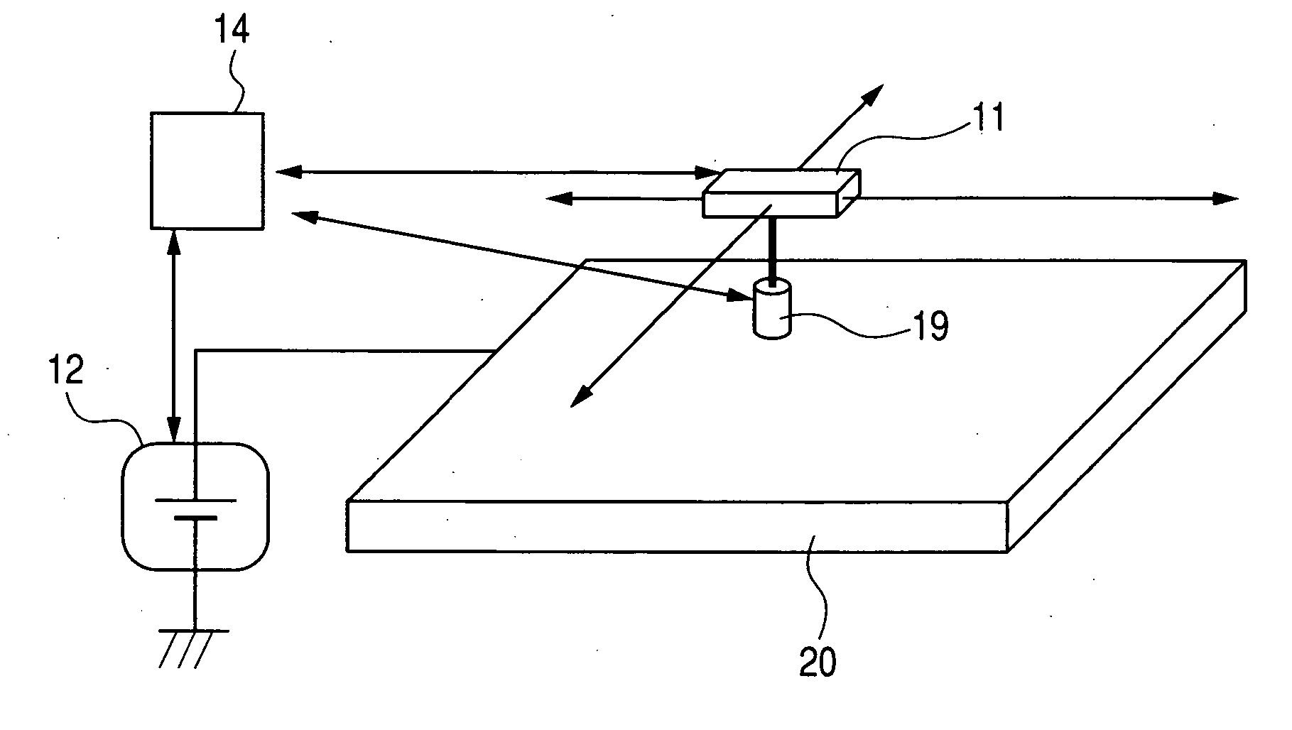
[0190] The anode electrode 10 was moved by the moving apparatus 11 to the detected position of the SE source, and the distance was set at Dr=0.2 mm. Then the voltage Vr of the high voltage source 12 was set according to a current of the ammeter 13. Vr is preferably a largest possible voltage lower than a discharge voltage of SE. Sin...
PUM
 Abstract
Description
Claims
Application Information
 - R&D
- Intellectual Property
- Life Sciences
- Materials
- Tech Scout
- Unparalleled Data Quality
- Higher Quality Content
- 60% Fewer Hallucinations
Browse by: Latest US Patents, China's latest patents, Technical Efficacy Thesaurus, Application Domain, Technology Topic, Popular Technical Reports.
© 2025 PatSnap. All rights reserved.Legal|Privacy policy|Modern Slavery Act Transparency Statement|Sitemap|About US| Contact US: help@patsnap.com