CMP pad having a streamlined windowpane

a windowpane and streamlined technology, applied in the field of polishing, can solve the problems of uneven point-to-point polishing rate across the wafer, scratches and other defects, and give a lot of results

Active Publication Date: 2006-03-23
ROHM & HAAS ELECTRONICS MATERIALS CMP HLDG INC
View PDF5 Cites 26 Cited by
  • Summary
  • Abstract
  • Description
  • Claims
  • Application Information

AI Technical Summary

Problems solved by technology

This is so because the disturbed flow thwarts an even distribution of polishing medium chemistry and uniform temperature field, contributing to non-uniformity in point-to-point polishing rates across the wafer.
In addition, the termination of many grooves at the edge of a blunt leading edge of a windowpane provides an opportunity for polish debris to accumulate, potentially leading to scratches and other defects.
None of the patents mentioned above, nor the designers of conventional CMP pad windowpanes appear to give much, if any, consideration to the effect of the plan-view shape of the windowpane on polishing nor the impact of the windowpane on polishing medium flow patterns in the pad-wafer gap, with the exception of flushness of the windowpane to the surrounding polishing surface.

Method used


Image

  • CMP pad having a streamlined windowpane
  • CMP pad having a streamlined windowpane
  • CMP pad having a streamlined windowpane

Examples


Embodiment Construction

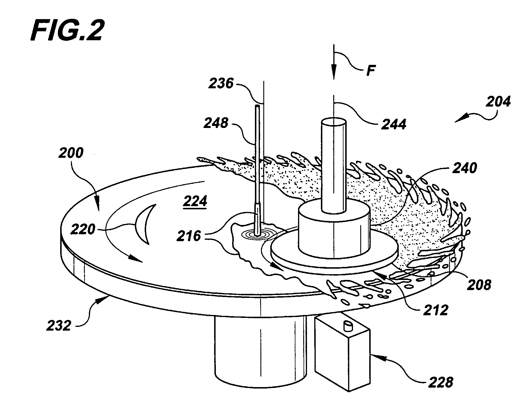
[0021] Referring again to the drawings, FIG. 2 generally illustrates a polishing pad 200 of the present invention in use with a dual-axis (CMP) polisher 204 that may be used to polish a surface 208 (hereinafter referred to as “polished surface”) of an article, such as wafer 212, in the presence of a polishing medium 216. Examples of other items that may be polished using polishing pad 200 include glass items, flat panel displays and magnetic information storage disks, among other workpieces. It is noted that for the sake of convenience, the term “wafer” is used below without the loss of generality. In addition, as used in this specification, including the claims, the term “polishing medium” includes particle-containing polishing solutions and non-particle-containing solutions, such as abrasive-free and reactive-liquid polishing solutions.

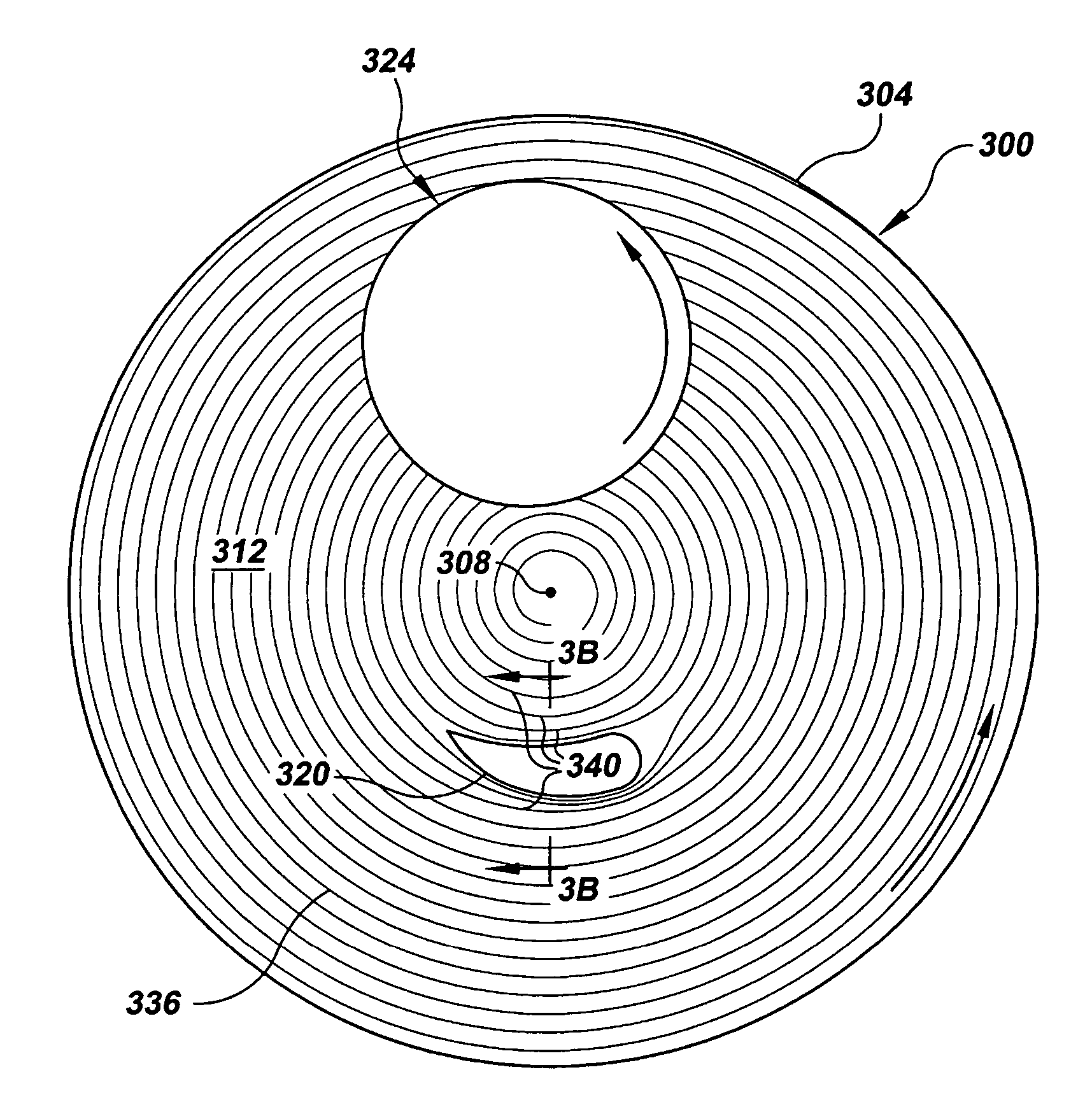
[0022] Polishing pad 200 is distinguished from prior art polishing pads by virtue of its inclusion of a windowpane 220 that is specifically shaped...


PUM


Abstract

A chemical mechanical polishing pad (200, 300, 400, 500, 600) that includes a translucent windowpane (220, 320, 404, 516, 524, 604) that allows optical measurements to be made using light energy reflected from the surface of a wafer (212, 324, 608) or other object being polished. The windowpane includes a trailing end (350, 416, 632) and a leading end (348, 412, 628) each having a streamlined shape so as to reduce the disturbance to the flow of a polishing medium (216) around the windowpane. The polishing pad may further include grooves (336, 428, 520, 640) that are diverted around the windowpane so as to provide a continuous path for the polishing medium in the region of the windowpane.

Description

[0001] This application is a continuation-in-part of application Ser. No. 10 / 946,864 filed Sep. 22, 2004.BACKGROUND OF THE INVENTION [0002] The present invention generally relates to the field of polishing. In particular, the present invention is directed to a CMP pad having a streamlined windowpane. [0003] In the fabrication of integrated circuits and other electronic devices, multiple layers of conducting, semiconducting and dielectric materials are deposited onto and etched from a surface of a semiconductor wafer. Thin layers of these materials may be deposited using any of a number of deposition techniques. Deposition techniques common in modern wafer processing include physical vapor deposition (PVD), also known as sputtering, chemical vapor deposition (CVD), plasma-enhanced chemical vapor deposition (PECVD) and electrochemical plating. Common etching techniques include wet and dry isotropic and anisotropic etching, among others. [0004] As layers of materials are sequentially d...

Claims


Application Information

Patent Timeline
Patent Type & Authority Applications(United States)
IPC IPC(8): B24B49/00B24D11/00B24B37/04
CPCB24B37/04B24D7/12B24B49/12
Inventor MULDOWNEY, GREGORY P.
Owner ROHM & HAAS ELECTRONICS MATERIALS CMP HLDG INC
Why Eureka
Try Eureka