Carbon nanotube-based electronic devices made by electrolytic deposition and applications thereof

an electronic device and carbon nanotube technology, applied in the field of carbon nanotube-based electronic devices, can solve the problems of lack of consensus in the industry, inability to speed up the process sufficiently to make billions of transistors practical, and inability to meet the needs of industrialization, etc., to achieve efficient and cost-effective effects

Inactive Publication Date: 2006-03-30
FOSTER-MILLER
View PDF12 Cites 75 Cited by
  • Summary
  • Abstract
  • Description
  • Claims
  • Application Information

AI Technical Summary

Benefits of technology

[0012] Furthermore, the fabrication method of the present invention provides an efficient, cost-effective process for mass producing nanotube-based electronic devices that is scalable.

Problems solved by technology

The semiconductor industry is facing increasingly difficult technological challenges, as it moves into the production of features at sizes below 100 nanometers.
Particular challenges are to achieve affordable scaling and achieve affordable lithography with dimensions below 100 nanometers, utilize new materials and structures, and achieve gigahertz frequency operations and very high device densities on chips.
There is a lack of consensus in the industry about how to solve the fabrication challenges that lie beyond the 100 nanometer barrier.
The problem confronting the industry is that the dominant technology used to make chips, optical lithography, uses light to form patterns on silicon.
Scanning probe methods have proven feasible for fabricating single devices one nanotube at a time, but no way has been found yet to speed up the process sufficiently to make billions of transistors practical.
The problem of combining different materials and assembling molecular electronic devices with specific features remains a significant challenge.
Those and other similar theoretical works outline the possibility to use carbon nanotubes as molecular devices, but fail to propose a design of such device and a method of its fabrication.
This work also fails to propose a design for carbon nanotube molecular electronic devices and a method of fabrication.

Method used


Image

  • Carbon nanotube-based electronic devices made by electrolytic deposition and applications thereof
  • Carbon nanotube-based electronic devices made by electrolytic deposition and applications thereof
  • Carbon nanotube-based electronic devices made by electrolytic deposition and applications thereof

Examples


Embodiment Construction

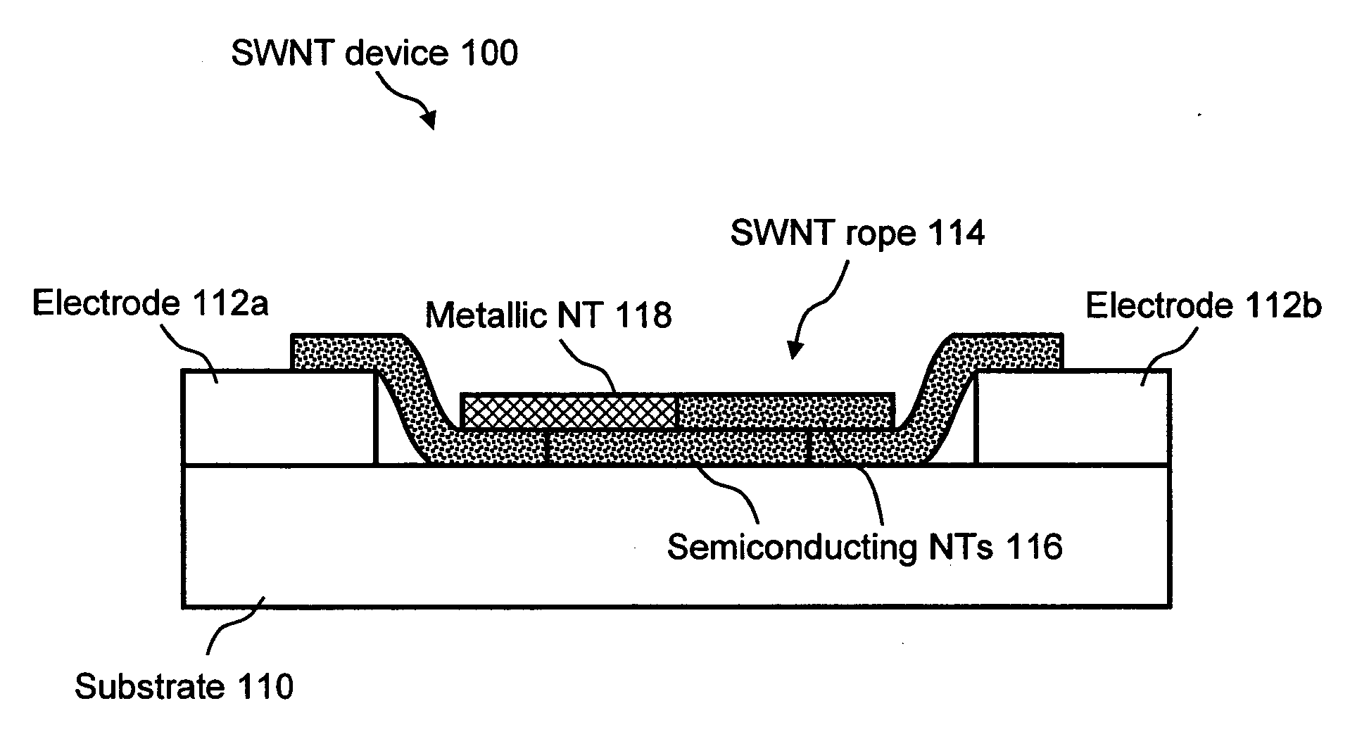
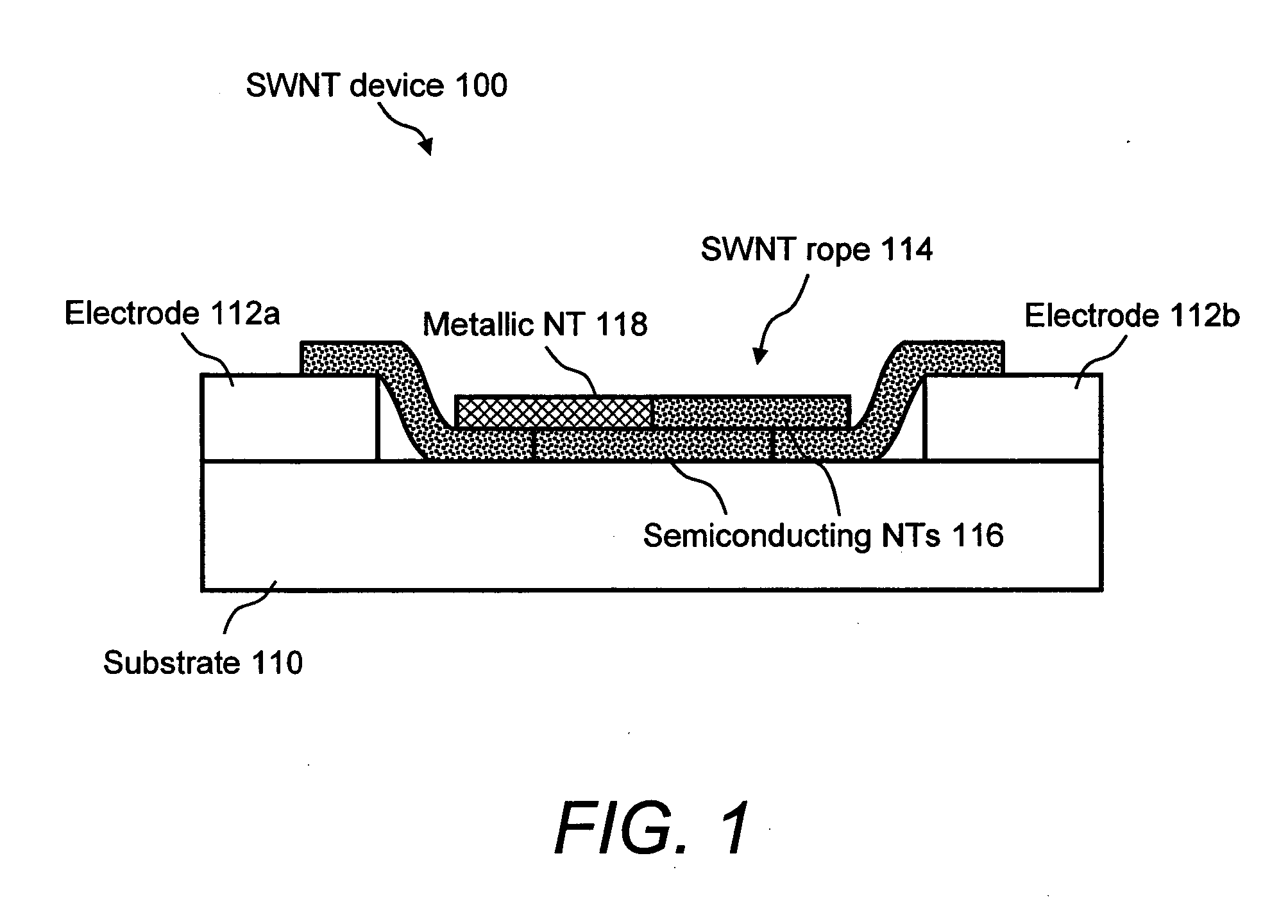
[0035]FIG. 1 illustrates a side view of a single-wall carbon nanotube (SWNT) device 100 (not drawn to scale) in its simplest form in accordance with a preferred embodiment of the invention. More specifically, the structure of SWNT device 100 includes a substrate 110, upon which is deposited a pair of electrodes 112, e.g., electrode 112a and electrode 112b. Additionally, an SWNT rope 114 is deposited upon substrate 110 between electrode 112a and electrode 112b and electrically connected thereto. SWNT rope 114 can be formed from a mixture of semiconducting nanotubes (NTs) 116 and isolated metallic NTs, such as metallic NT 118. Semiconducting nanotubes NTs 116 are carbon nanotubes that exhibit typical semiconductor current-voltage behavior and metallic NTs 118 are carbon nanotubes that exhibit ohmic current-voltage behavior. Single nanotubes which are semiconductive can also be used to form this device.

[0036] Substrate 110 can be formed from any electrically non-conductive material th...


PUM

PropertyMeasurementUnit
sizesaaaaaaaaaa
wavelengthaaaaaaaaaa

Abstract

Carbon nanotube-based devices made by electrolytic deposition and applications thereof are provided. In a preferred embodiment, the present invention provides a device comprising at least one array of active carbon nanotube junctions deposited on at least one microelectronic substrate. In another preferred embodiment, the present invention provides a device comprising a substrate, at least one pair of electrodes disposed on the substrate, wherein one or more pairs of electrodes are connected to a power source, and a bundle of carbon nanotubes disposed between the at least one pair of electrodes wherein the bundle of carbon nanotubes consist essentially of semiconductive carbon nanotubes. In another preferred embodiment, a semiconducting device formed by electrodeposition of carbon nanotubes between two electrodes is provided. The invention also provides preferred methods of forming a semiconductive device by applying a bias voltage to a carbon nanotube rope. The plurality of metallic single-wall carbon nanotubes are removed (e.g., by application of bias voltage) in an amount sufficient to form the semiconducting device. The devices of the invention include, but not limited to, chemical or biological sensors, carbon nanotube field-effect transistors (CNFETs), tunnel junctions, Schottky junctions, and multi-dimensional nanotube arrays.

Description

CROSS-REFERENCES TO RELATED APPLICATIONS [0001] This application claims priority to U.S. Provisional Patent Application No. 60 / 557,118 filed on Mar. 26, 2004 which is hereby incorporated by reference in its entirety.STATEMENT REGARDING FEDERALLY SPONSORED RESEARCH OR DEVELOPMENT [0002] The United States Government may have certain rights in this invention pursuant to Grant Numbers F19628-03-C-0075 and N41756-02-M-1043.FIELD OF THE INVENTION [0003] The present invention relates to carbon nanotube-based electronic devices. In particular, this invention relates to carbon nanotube-based electronic devices made by electrolytic deposition. BACKGROUND OF THE INVENTION [0004] The semiconductor industry is facing increasingly difficult technological challenges, as it moves into the production of features at sizes below 100 nanometers. Particular challenges are to achieve affordable scaling and achieve affordable lithography with dimensions below 100 nanometers, utilize new materials and stru...

Claims


Application Information

Patent Timeline
Patent Type & Authority Applications(United States)
IPC IPC(8): H01L29/06H01L51/00H01L51/10
CPCB82Y10/00H01L51/0048H01L51/102H01L51/0595H01L51/0052Y10S977/888H10K85/221H10K85/615H10K10/701H10K10/82H10K19/00H10K71/125H10K71/311H10K30/671H10K50/00
Inventor TIANO, THOMASGANNON, JOHNCAREY, CHARLESFARRELL, BRIANCZERW, RICHARD
Owner FOSTER-MILLER
Why Eureka
Try Eureka