
Vertical alignment active matrix liquid crystal display device

a liquid crystal display and active matrix technology, applied in non-linear optics, instruments, optics, etc., can solve the problems of large view angle dependency of contrast, poor view angle characteristic, display unevenness or irregularity, etc., and achieve the effect of wide view angle without display unevenness

Inactive Publication Date: 2006-03-30
CASIO COMPUTER CO LTD
View PDF69 Cites 23 Cited by
  • Summary
  • Abstract
  • Description
  • Claims
  • Application Information

AI Technical Summary

Benefits of technology

[0014] It is an object of the present invention is to provide a liquid crystal display device which has bright display and a wide view angle without display unevenness.
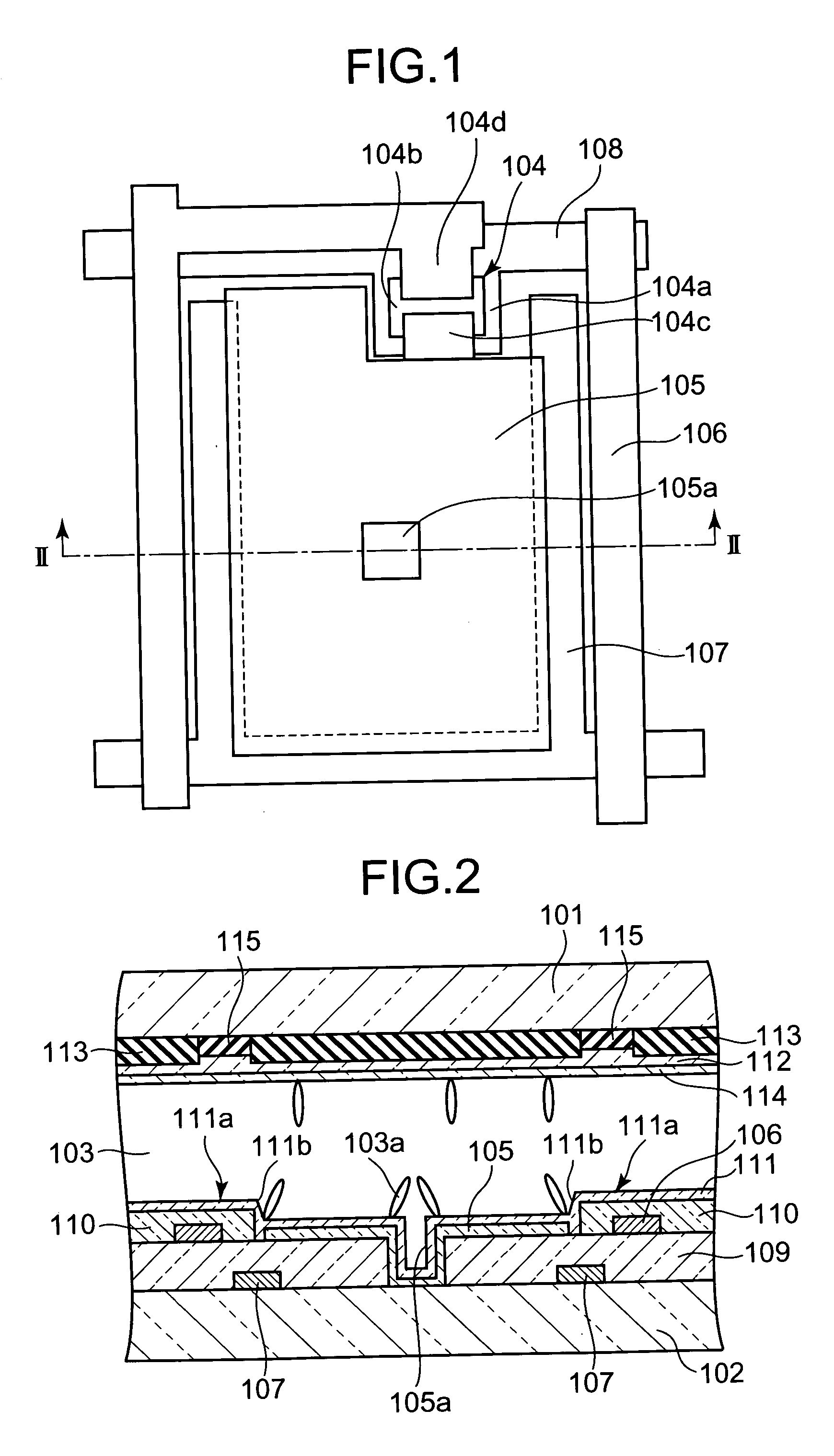
[0022] In the liquid crystal display device according to the first aspect, the recess portion or the projecting portion, which is formed on at least one of the first and second electrodes, tilts the liquid crystal molecules in the vicinity of the recess portion or the projecting portion so as to face the center of the pixel, so that the liquid crystal molecules at the peripheral portion of the pixel region is tilted toward the center of the pixel by the horizontal electric field that is generated between the second electrode and the auxiliary electrode. Therefore, a monodomain where the liquid crystal molecules are aligned spirally toward the center of the pixel region from the peripheral portion of the pixel is formed for each pixel region, and the spiral center of the alignment of the liquid crystal molecules becomes steady over the entire pixel regions. This provides a stable and uniform aligned state, thus suppressing the occurrence of display unevenness.
[0043] According to the liquid crystal display device of the third aspect, as at least one of the first and second electrodes is formed tilted toward the peripheral portion from the center of each pixel region, the liquid crystal molecules are aligned spirally toward the center of each pixel region from the peripheral portion thereof, thus making the aligned state of the liquid crystal molecules in each pixel region stable.

Problems solved by technology

This results in a large view angle dependency of the contrast and a poor view angle characteristic.
This causes display unevenness or irregularity.

Method used


Image

  • Vertical alignment active matrix liquid crystal display device
  • Vertical alignment active matrix liquid crystal display device
  • Vertical alignment active matrix liquid crystal display device

Examples


first embodiment

[0057]FIG. 1 is a top plan view schematically illustrating one pixel structure of a vertical alignment liquid crystal display device according to the first embodiment of the invention. FIG. 2 is a cross-sectional view of one pixel illustrated in FIG. 1 cut along the line II-II. In FIG. 2, liquid crystal molecules are represented by long ellipses as a model.

[0058] The liquid crystal display device comprises a pair of glass substrates 101 and 102, arranged opposite to each other, and a liquid crystal 103 with the negative dielectric anisotropy, filled between one glass substrate 102 (hereinafter called TFT substrate 102) and the other glass substrate 101 (hereinafter called opposing substrate 101).

[0059] Formed on the surface of the TFT substrate 102 opposing the opposing substrate 101 are TFT devices 104, pixel electrodes 105, drain lines 106, auxiliary electrodes 107, gate lines 108, a gate insulation film 109, an insulation film 110, and an alignment film 111. Formed on the inner...

second embodiment

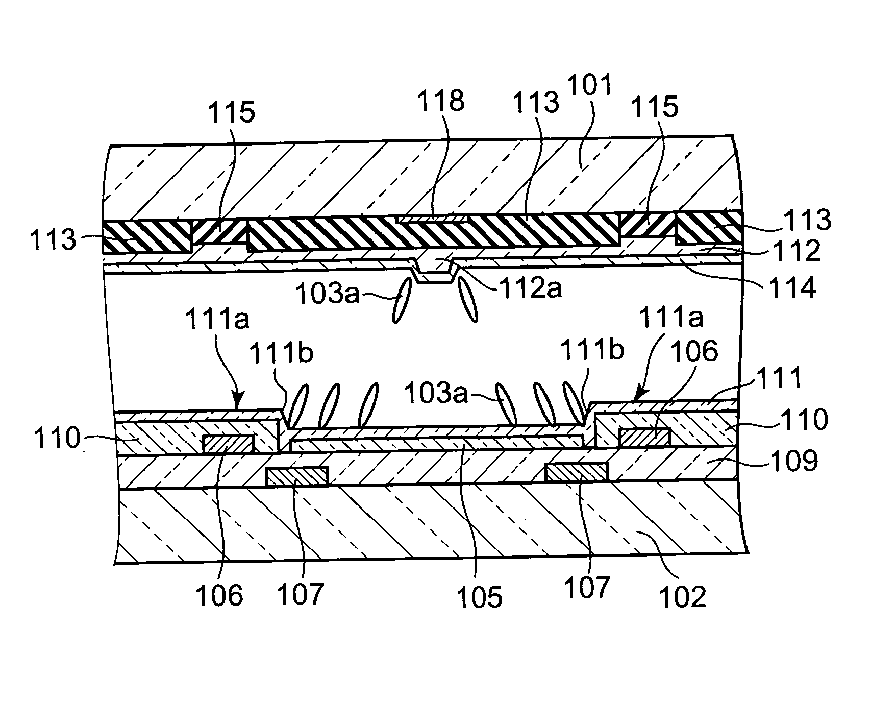
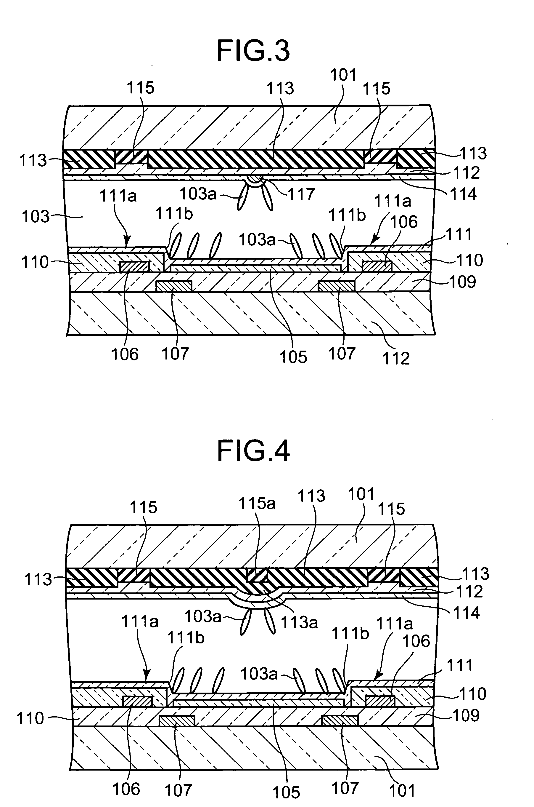
[0079] The second embodiment of the invention will be explained referring to FIG. 3.

[0080]FIG. 3 illustrates the pixel structure of a liquid crystal display device according to the second embodiment.

[0081] In FIG. 3, formed on the inner surface of the TFT substrate 102 are the TFT devices 104, the pixel electrodes 105, the drain lines 106, the auxiliary electrodes 107, the gate lines 108, the gate insulation film 109, the insulation film 110, and the alignment film 111. The opposing electrode 112, the color filter 113, the alignment film 114, and the black mask 115 are formed on the inner surface of the opposing substrate 101. In the embodiment, the same constituting elements as those of the first embodiment will be denoted by the same reference numbers to avoid repeating their otherwise redundant descriptions.

[0082] In the embodiment, the color filter 113 is formed by coating a color resist solution of acrylic resin and exposing the resultant resist film in a pattern, and develo...

third embodiment

[0093] In the liquid crystal display device according to the invention, the above-described projecting portion in the second embodiment may be a spacer formed by patterning a transparent resin material on the opposing electrode.

[0094] In a liquid crystal display device according to the third embodiment of the invention, as shown in FIG. 6, a spacer 119 is formed like a cone with an inclined side, and the alignment film 114 is so formed as to cover the spacer 119. As the third embodiment is identical to the second embodiment in structure except for the spacer 119, the same constituting elements as those of the second embodiment will be denoted by the same reference numbers to avoid repeating otherwise redundant descriptions.

[0095] According to the third embodiment, when a voltage is applied between the opposing electrode 112 and the pixel electrodes 105, the liquid crystal molecules 103a are influenced by the inclined side of the spacer 119 and aligned radially around the spacer 11...


PUM


Abstract

A liquid crystal display device comprises a TFT substrate where TFTs are formed, an opposing substrate (CF substrate), a liquid crystal with a negative dielectric anisotropy filled between both substrates, a pixel electrode, and an auxiliary electrode formed around the pixel electrode. The pixel electrode has a recess portion formed by etching a gate insulation film. The liquid crystal molecules are aligned tilted toward the center of a pixel according to the shape of the recess portion.

Description

BACKGROUND OF THE INVENTION [0001] 1. Field of the Invention [0002] The present invention relates to a vertical alignment active matrix liquid crystal display device whose liquid crystal molecules are aligned vertical to the surface of a substrate. [0003] 2. Description of the Related Art [0004] A conventional TFT liquid crystal panel comprises a TFT (Thin Film Transistor) substrate on which TFTs and pixel electrodes and the like are formed, a CF (Color Filter) substrate on which color filters and an opposing electrode are formed, and a liquid crystal layer which is sandwiched between those substrates. A TFT liquid crystal display panel which has liquid crystal molecules homogeneously aligned, such as a TN (Twisted Nematic) liquid crystal display device, uses a material with a positive dielectric anisotropy. A TFT liquid crystal display panel which has liquid crystal molecules homeotropically aligned uses a material with a negative dielectric anisotropy, and aligns the director (mol...

Claims


Application Information

Patent Timeline
IPC IPC(8): G02F1/1337
CPCG02F1/133371G02F2001/133742G02F1/133707G02F1/133742G02F1/1337
Inventor MIZUSAKO, RYOTAYAMAGUCHI, MINORUNAKAJIMA, YASUSHI
Owner CASIO COMPUTER CO LTD
Learn More