Defect detection apparatus and defect detection method

a technology of defect detection and defect detection, applied in the field of defect detection apparatus and defect detection method, can solve the problems of long time for operator or other apparatus to check (review), short circuit, and low efficiency of defect detection, and achieve the effect of high efficiency

Inactive Publication Date: 2006-03-30
DAINIPPON SCREEN MTG CO LTD
View PDF13 Cites 63 Cited by
  • Summary
  • Abstract
  • Description
  • Claims
  • Application Information

AI Technical Summary

Benefits of technology

[0007] The present invention is intended for a defect detection apparatus for detecting defects of a pattern formed on a substra

Problems solved by technology

In a case where a very fine and dense wiring pattern is formed, for example, even a defect whose size (area) corresponds to one pixel or so may be critical, causing a short circuit, an open or the like in interconnection.
In a case where such a dense pattern and a sparse pattern are mixed in a target image, even if the

Method used


Image

  • Defect detection apparatus and defect detection method
  • Defect detection apparatus and defect detection method
  • Defect detection apparatus and defect detection method

Examples


Embodiment Construction

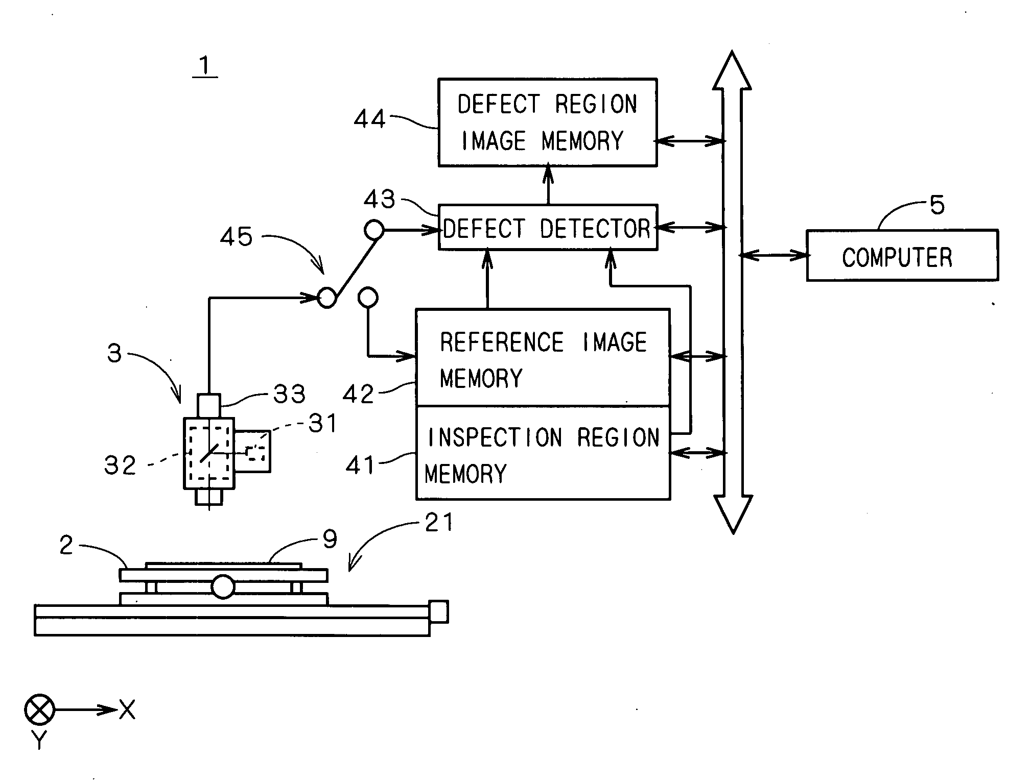
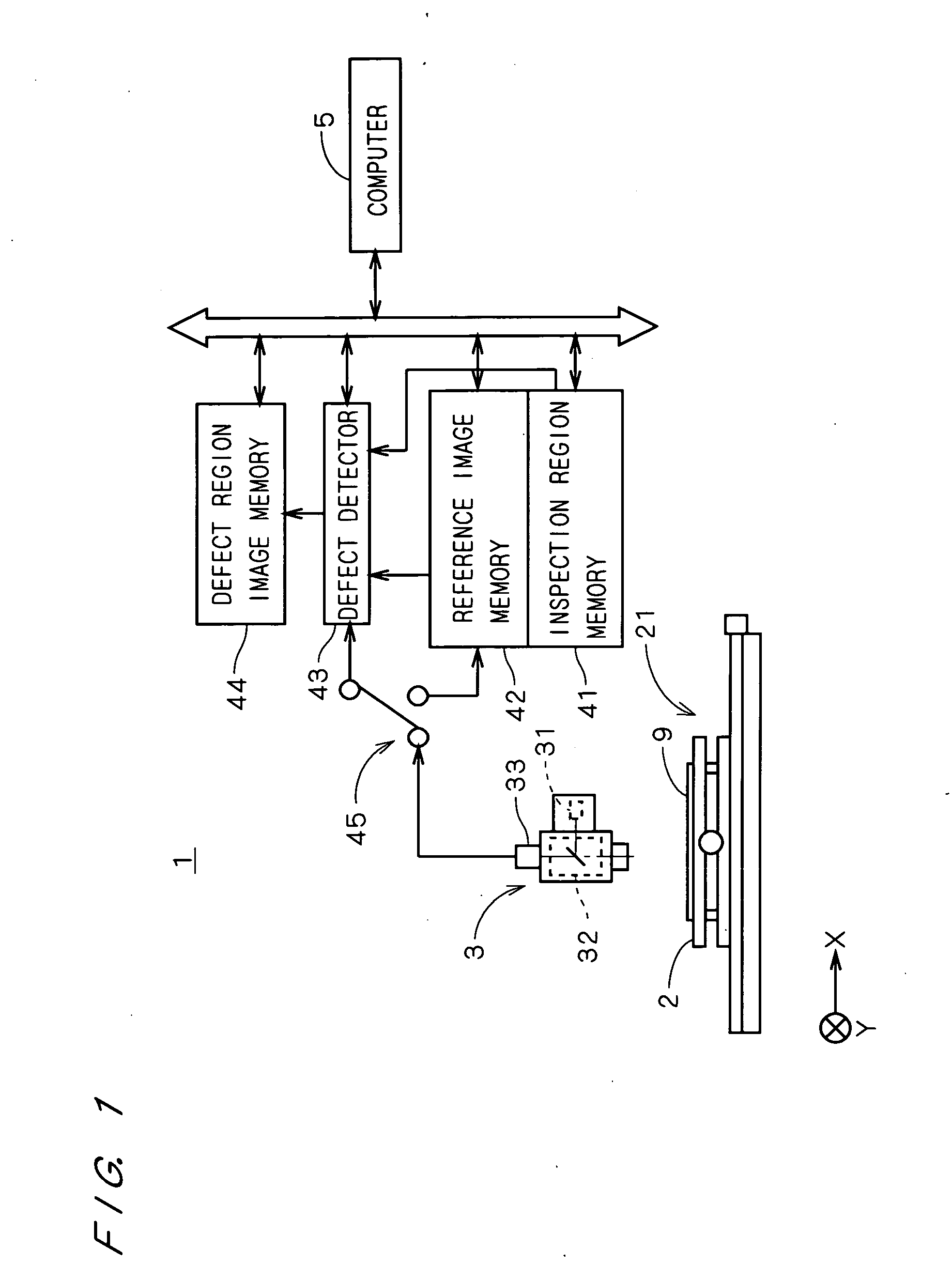
[0031]FIG. 1 is a view showing a construction of a defect detection apparatus 1 in accordance with the first preferred embodiment of the present invention. The defect detection apparatus 1 comprises a stage 2 for holding a semiconductor substrate 9 on which a predetermined wiring pattern is formed, an image pickup part 3 for picking up an image of the substrate 9 to acquire a grayscale image of the substrate 9 and a stage driving part 21 for moving the stage 2 relatively to the image pickup part 3.

[0032] The image pickup part 3 has a lighting part 31 for emitting an illumination light, an optical system 32 which guides the illumination light to the substrate 9 and receives the light from the substrate 9 and an image pickup device 33 for converting an image of the substrate 9 formed by the optical system 32 into an electrical signal, and the image pickup device 33 outputs image data of the substrate 9. The stage driving part 21 has mechanisms for moving the stage 2 in the X directio...


PUM


Abstract

A defect detection apparatus (1) comprises an image pickup part (3) for picking up an image of a substrate (9) to acquire a grayscale target image, from which pixel values of the target image are sequentially outputted to a defect detector (43). The defect detector (43) compares the target image with a reference image to generate a defect region image representing regions of defects included in a plurality of predetermined inspection regions, to be stored in a defect region image memory (44). A computer (5) obtains an area and a barycentric position of each of the defects in the defect region image to specify an inspection region including the defect and performs limitation (i.e., selection) of defects on the basis of a defect detection condition set for each inspection region on the area of defect. It is possible to detect defects with high efficiency by using a defect detection condition on a different area of defect for each inspection region.

Description

BACKGROUND OF THE INVENTION [0001] 1. Field of the Invention [0002] The present invention relates to a technique for detecting defects of a pattern formed on a substrate. [0003] 2. Description of the Background Art [0004] In a field of inspecting a pattern formed on a semiconductor substrate, a glass substrate, a printed circuit board, or the like (hereinafter, referred to as “substrate”), conventionally, a comparison check method has been used. For example, from a grayscale target image to be inspected and a grayscale reference image, a differential absolute value image representing absolute values of differences in pixel value between these images is obtained and each of pixels in this image is binarized by a predetermined threshold value, to detect a region specified on a pixel basis as a defect. [0005] Japanese Patent Application Laid Open Gazette No. 11-135583 (Document 1) discloses a method for detecting a defect with high accuracy with detection sensitivity in accordance with...

Claims


Application Information

Patent Timeline
IPC IPC(8): G06K9/00
CPCG06T2207/30148G06T7/001H01L22/00
Inventor ONISHI, HIROYUKI
Owner DAINIPPON SCREEN MTG CO LTD
Why Eureka
Try Eureka