Film forming condition determination method, film forming method, and film structure manufacturing method

a technology of condition determination and film, applied in the direction of semiconductor/solid-state device testing/measurement, instruments, nuclear elements, etc., can solve the problems of requiring a lot of time and work, affecting the production efficiency of prototype products, and rarely obtaining prototype products having the same characteristics as prototypes, etc., to reduce the production of mass-production prototypes, reduce labor and burden concerning analysis, and control the generation of accompanying dielectric films more easily

Inactive Publication Date: 2006-03-30
HORIBA LTD
View PDF1 Cites 24 Cited by
  • Summary
  • Abstract
  • Description
  • Claims
  • Application Information

AI Technical Summary

Benefits of technology

[0020] Another object of the invention is to provide a film forming method capable of significantly reducing the time and the work required to shift a film structure from a prototype stage to a mass-production stage.
[0053] In the ninth aspect, by using the above-mentioned film forming condition determination method to specify a film forming condition variable, it is possible to specify efficiently a film forming condition variable that can make the film characteristic of a film structure, formed by the second film forming apparatus closer to the film characteristic of the film structure, formed by the first film forming apparatus, and it is therefore possible to shift smoothly to the mass-production stage.

Problems solved by technology

However, since a film forming apparatus for manufacturing the prototype and a film forming apparatus for mass-production in the factory differ in the scale, etc., even if the film forming conditions, optimized for the film forming apparatus for prototype are applied, as it is, to the film forming apparatus in the factory, products having the same characteristics as the prototype are rarely obtained.
The above-described conventional electrical measurement has the problem that it takes a lot of time and work.
In other words, in order to perform the measurement, first a plurality of film structures to be measured are prepared, and then probing or wire bonding is performed, after creating an electrode part for each film structure, and thus a lot of time and work are required.
Note that if the electrode part is once formed on the film structure, the electrode part can never be removed, and therefore it is difficult to effectively use the film structure used for the measurement.
Moreover, determining an optimal film forming condition, by evaluating a plurality of measurement results, creates a heavy labor burden, and particularly if the number of kinds of parameters concerning the film forming condition of a film structure to be manufactured is large, the same number of electrical measurements and the evaluation process are required for each kind, and consequently the labor burden increases.
However, since the number of objects to be measured and evaluated at the mass-production stage is much larger compared to the prototype stage, there is the problem that a lot of time and work are necessary to shift to the mass-production stage as well.
Furthermore, after shifting to the mass-production stage, it is physically impossible to form an electrode part after deposition of each intermediate film structure, and perform electrical measurement by probing or wire bonding, therefore, presently, a product inspection is performed on a finished film structure, obtained through a plurality of film forming steps.
Thus, since an intermediate film structure, that may contain a defective layer, during any step of a film forming process, flows to the final film forming step, and as a result, a lot of steps are performed wastefully, an improvement of the yield is not achieved.
Since the methods of Japanese Patent Applications Laid-Open No. 2002-289614 and No. 2001-126324 do not take into account the shift to the mass-production stage and an improvement of the yield at the mass-production stage, even if the methods disclosed in Japanese Patent Applications Laid-Open No. 2002-289614 and No. 2001-126324 are applied, the above-mentioned problems cannot be solved.
Moreover, the measurement and analysis by a transmission electron microscope (TEM) require even more work, compared with electrical measurement, and the degree of difficulty of the measurement is high.
Therefore, even if the transmission electron microscope (TEM) is used, the above-mentioned problem cannot be solved.
Although the presence of such an accompanying film is detected by electrical measurement, the single electrical measurement can not determine the characteristic of the accompanying film and the characteristic of the high-dielectric constant film or ferroelectric film separately.
However, it has not yet been established, how the dielectric constant of the accompanying film varies with a change in the film forming conditions, and there is a possibility, that the accompanying film may loose the characteristic of the high-dielectric constant substance or ferroelectric substance, when the dielectric constant of the accompanying film is low.
However, even when the methods of Japanese Patent Applications Laid-Open No. 2002-289614 and No. 2001-126324 are used, it is impossible to determine a film forming conditions capable of controlling the generation of the accompanying film.

Method used


Image

  • Film forming condition determination method, film forming method, and film structure manufacturing method
  • Film forming condition determination method, film forming method, and film structure manufacturing method
  • Film forming condition determination method, film forming method, and film structure manufacturing method

Examples


first embodiment

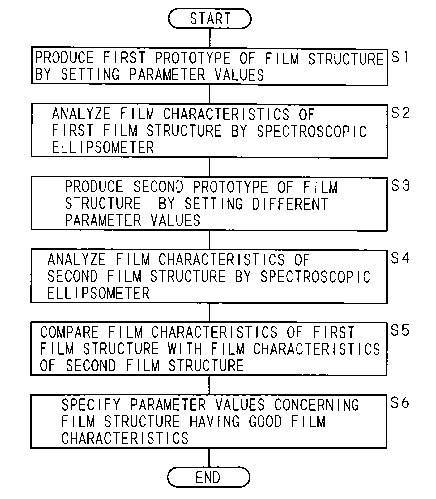
[0072]FIG. 1 is a flowchart showing the processing steps of a film forming condition determination method, according to the present invention. The present invention is a method for determining a film forming condition, in forming a high-dielectric constant film or ferroelectric film as a dielectric film with a dielectric constant of not lower than 50, based on electrical measurement, on a substrate (for example, with a deposited material for electrode), and more particularly for determining a film forming condition, capable of forming a film structure, including an intended high-dielectric constant film or ferroelectric film, by reducing an accompanying dielectric film, that is generated at the interface between the substrate and the high-dielectric constant film or ferroelectric film, with the formation of the high-dielectric constant film or ferroelectric film.

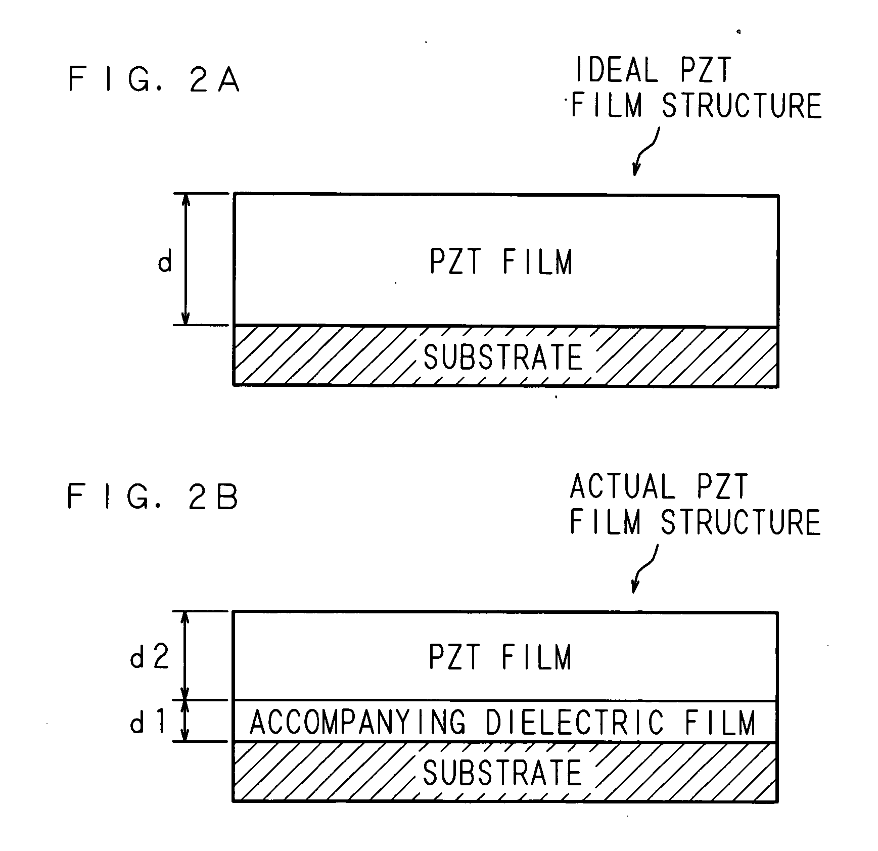
[0073] The first embodiment illustrates, as shown in FIG. 2A, the case where a single PZT (lead zirconate titanate) film, ...

embodiment 1

[0099] For the determination as to whether or not the film structure has good film characteristics, a determination may be made that accompanying dielectric film with a thinner film thickness d1 has good film characteristic, based only on the film thickness d1 as the characteristic of the accompanying dielectric film, or a determination may be made that the PZT film with a thicker film thickness d2 and a film characteristic (such as a dielectric constant) closer to the intended value has good film characteristic, based on the film thickness d2 and the film characteristic as the characteristics of the PZT film. Further, the film forming condition determination method may also be applied to determine a film forming condition of high dielectric or ferroelectric other than PZT, and may also be applied, for example, to form a PLZT film.

[0100] Although the determination of the film forming condition was explained with the respect to the accompanying dielectric film, generated at the inte...

second embodiment

[0111] If a film forming apparatus, for use in the mass-production stage, is a MOCVD apparatus, for example, its basic structure is the same, as the one shown in FIG. 3, but it is capable of accepting a plurality of substrates S on the mount base 6, so that a plurality of film structures can be formed by one film forming processing. Therefore, since the film forming apparatus for mass-production differs in the scale from the film forming apparatus used in the prototype production stage, an adjustment is made, using the film forming method of the present invention to match the film forming condition determined at the prototype production stage with the mass-production stage. Note that the film forming method of the second embodiment is applicable to both the film formation of a high dialectic film or ferroelectric film, such as PZT, whose dielectric constant based on electrical measurement is not lower than 50, and the film formation of a dielectric film, with a dielectric constant l...


PUM

PropertyMeasurementUnit
dielectric constantaaaaaaaaaa
thickness d1aaaaaaaaaa

Abstract

Among a plurality of parameters concerning a film forming condition, different parameter values are set for one parameter and the same predetermined values are set for other parameters to manufacture two pieces of film structures including a high-dielectric constant film or ferroelectric film formed on a substrate. The film characteristics of the respective film structures are analyzed by a spectroscopic ellipsometer, a film structure in which the ratio of the presence of an accompanying dielectric film is smaller, is determined to be good by comparing the analysis results, and a parameter value set for the manufacture of the good film structure is determined. Then similar processing is performed, to specify an optimal parameter value for one parameter, and similar processing is also performed for other parameters to specify an optimal parameter value for the other parameters.

Description

CROSS-REFERENCE TO RELATED APPLICATION [0001] This non-provisional application claims priority under 35 U.S.C. §119(a) on Patent Application No. 2004-280568 filed in Japan on Sep. 27, 2004, the entire contents of which are hereby incorporated by reference.BACKGROUND OF THE INVENTION [0002] 1. Field of the Invention [0003] The present invention relates to a film forming condition determination method capable of controlling the state of generation of an accompanying dielectric film that is generated with the formation of high-dielectric constant film or ferroelectric film, and efficiently determining an optimal film forming condition, for making the film structure closer to an intended film structure, relates to a film forming method capable of shifting smoothly a prototype of film structure to a mass-production stage, and further relates to a film structure manufacturing method capable of realizing an improvement in the yield, when mass-producing the film structure. [0004] 2. Descrip...

Claims


Application Information

Patent Timeline
Patent Type & Authority Applications(United States)
IPC IPC(8): H01L21/66G01R31/26
CPCC23C16/52G01B11/0641H01L28/56H01L21/31691G01N21/211H01L21/02197
Inventor FUNAKUBO, HIROSHIHONDA, YOSHIHISANABATOVA-GABAIN, NATALIYATERAI, ASUKA
Owner HORIBA LTD
Why Eureka
Try Eureka