Memory devices including barrier layers and methods of manufacturing the same

Active Publication Date: 2006-04-13
SAMSUNG ELECTRONICS CO LTD
View PDF2 Cites 12 Cited by
  • Summary
  • Abstract
  • Description
  • Claims
  • Application Information

AI Technical Summary

Benefits of technology

[0008] Example embodiments of the present invention provide memory devices (e.g., nonvolatile memory devices), which may be st

Problems solved by technology

If power is interrupt

Method used


Image

  • Memory devices including barrier layers and methods of manufacturing the same
  • Memory devices including barrier layers and methods of manufacturing the same
  • Memory devices including barrier layers and methods of manufacturing the same

Examples


Embodiment Construction

[0026] Memory devices (e.g., nonvolatile memory devices), which may include a tunneling barrier layer (e.g., a multilayered tunneling barrier layer) and methods of manufacturing the same according to example embodiments of the present invention will now be described with reference to the accompanying drawings.

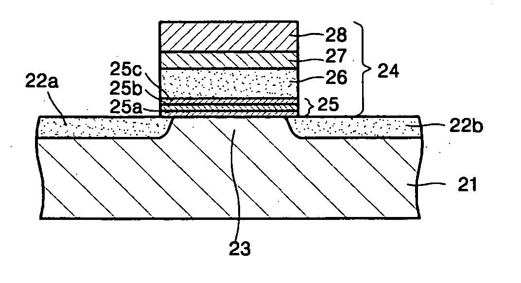
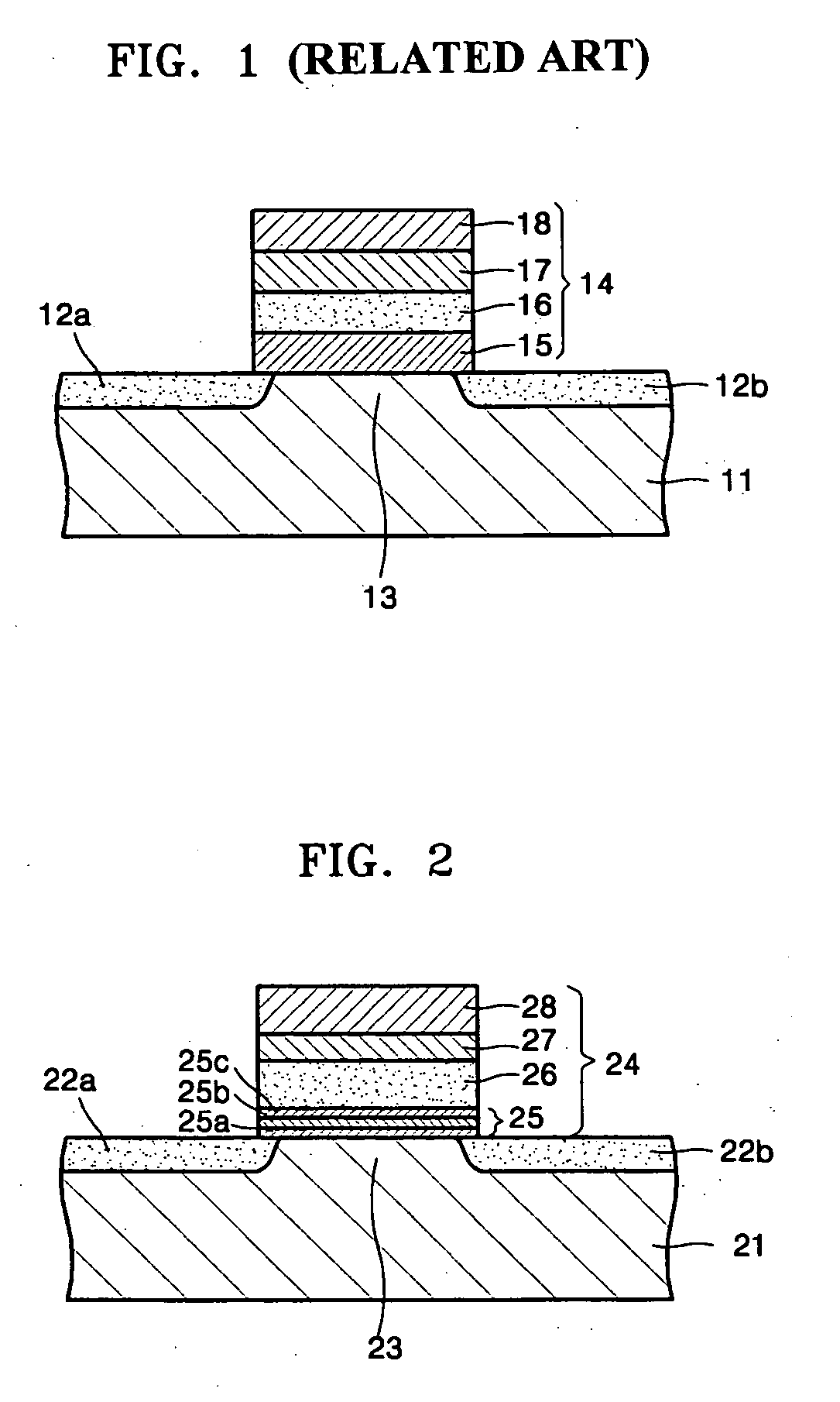
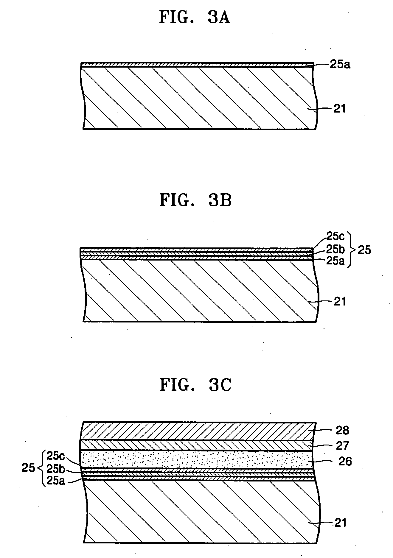
[0027]FIG. 2 is a cross sectional view of a memory device (e.g., a nonvolatile memory device) according to an example embodiment of the present invention. The memory device of FIG. 2 may include a barrier layer (e.g., a barrier layer structure and / or a multilayered tunneling barrier layer) in accordance with another example embodiment of the present invention.

[0028] Referring to FIG. 2, a source region 22a and a drain region 22b may be implanted with dopant (e.g., impurities). The source region 22a and / or the drain region 22b may be prepared in, or on, a substrate 21 (e.g., semiconductor substrate). A channel region 23 may be formed in, or on, the substrate 21, for example, b...


PUM


Abstract

Memory devices and methods of manufacturing the same are provided. Memory devices may include a substrate, a source region and a drain region and a gate structure. The gate structure may be in contact with the source and drain regions, and may include a barrier layer. The barrier layer may be formed of at least two layers. The at least two layers may have different bandgap energies.

Description

PRIORITY STATEMENT [0001] This application claims priority under 35 U.S.C. §119 of Korean Patent Application No.10-2004-0080353, filed on Oct. 8, 2004, in the Korean Intellectual Property Office (KIPO), the entire contents of which are incorporated herein by reference. BACKGROUND OF THE INVENTION [0002] 1. Field of the Invention [0003] Example embodiments of the present invention relate to memory devices (e.g., nonvolatile memory devices), which may include at least one barrier (e.g., multilayered tunneling barrier) and methods of manufacturing the same. For example, in one or more example embodiments of the present invention, a tunneling barrier layer may be formed in a nonvolatile memory device using a plurality of dielectric layers and methods of manufacturing the same. The dielectric layers may have different bandgap energies. [0004] 2. Description of the Related Art [0005] A semiconductor memory device may be a volatile memory device or a nonvolatile memory device. A volatile m...

Claims


Application Information

Patent Timeline
IPC IPC(8): G11C7/00
CPCH01L21/28273H01L29/513H01L29/7881H01L29/40114H01L21/823437
Inventor JEON, SANG-HUNKIM, CHUNG-WOOHWANG, HYUN-SANG
Owner SAMSUNG ELECTRONICS CO LTD
Why Eureka
Try Eureka