Multilayer circuit board

Inactive Publication Date: 2006-04-20
PANASONIC CORP
View PDF10 Cites 39 Cited by
  • Summary
  • Abstract
  • Description
  • Claims
  • Application Information

AI Technical Summary

Benefits of technology

[0007] In order to cope with the above-stated problems, it is an object of the present invention to provide a multilayer

Problems solved by technology

Therefore, if an inductance larger than a predetermined threshold value is required, it may be difficult to increase the winding number.
Also, when the number of the layers of the board is increased for obtaining a larger inductance, displacement in the lamination may occur.
In an extreme case, the connection of build-up vias with coil patterns formed between the layers may become unstable, resulting in electrical discontinuity.
However, since the board is a so-called double-sided circuit board including a single layer of an electrical insulative base member and conductive patterned

Method used


Image

  • Multilayer circuit board
  • Multilayer circuit board
  • Multilayer circuit board

Examples


embodiment 1

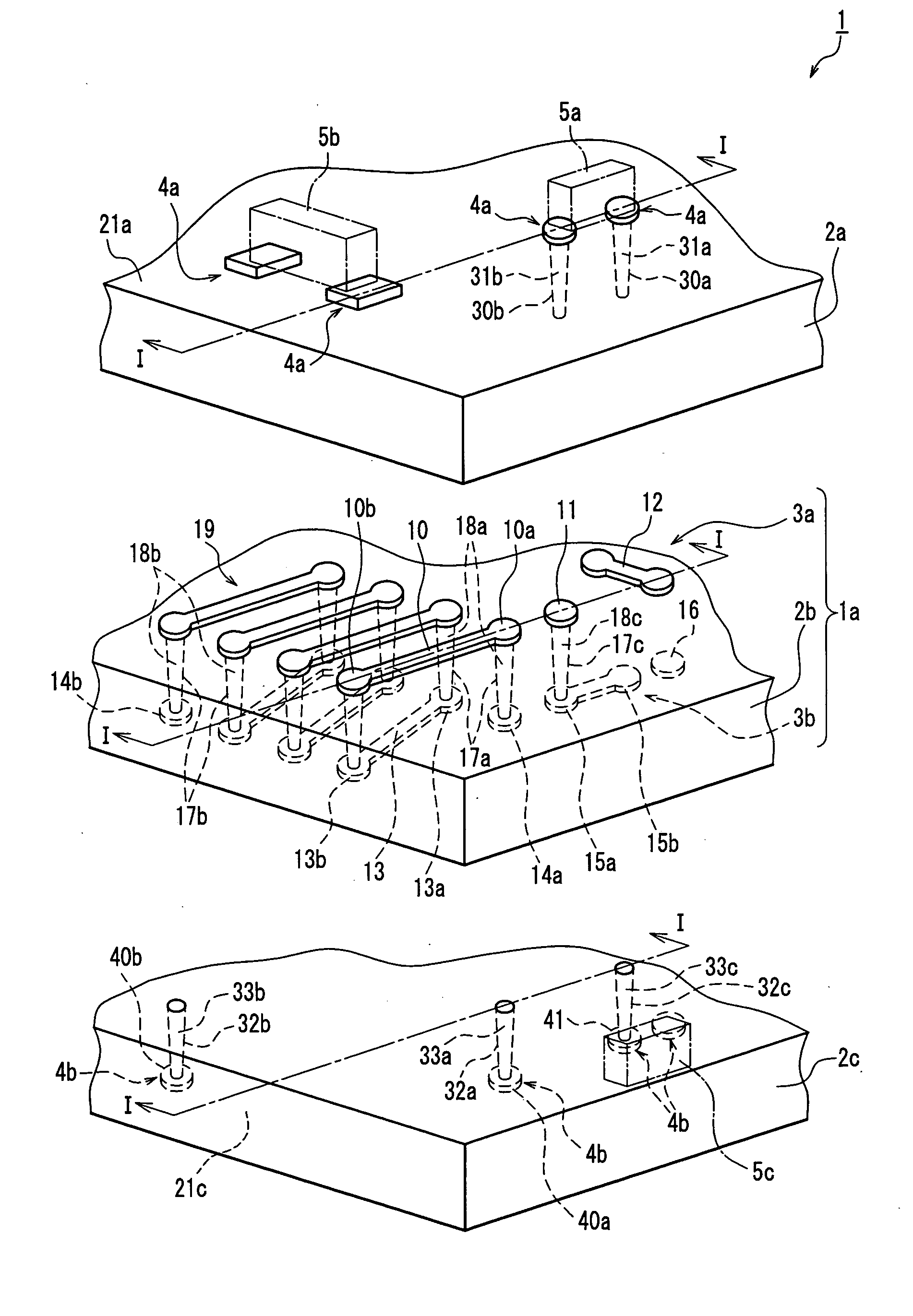
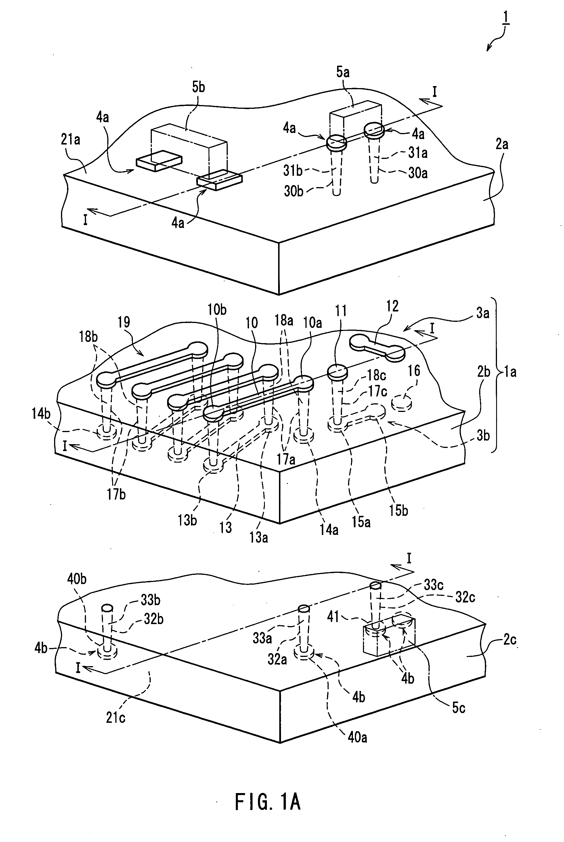
[0032] Firstly, Embodiment 1 of the present invention will be described below, with reference to the drawings as needed. FIG. 1A to be referred to in the following is a perspective view of a multilayer circuit board according to Embodiment 1 of the present invention, showing each layer separately, and FIG. 1B is a cross-sectional view of the multilayer circuit board according to Embodiment 1 taken along the line I-I of FIG. 1A.

[0033] As shown in FIGS. 1A and 1B, a multilayer circuit board 1 according to Embodiment 1 of the present invention includes: electrical insulative base members 2a, 2b and 2c; a conductive patterned layer 3a provided between the electrical insulative base member 2a and the electrical insulative base member 2b; a conductive patterned layer 3b provided between the electrical insulative base member 2b and the electrical insulative base member 2c; and conductive patterned layers 4a and 4b respectively provided on outer surfaces 21a and 21c of the electrical insul...

embodiment 2

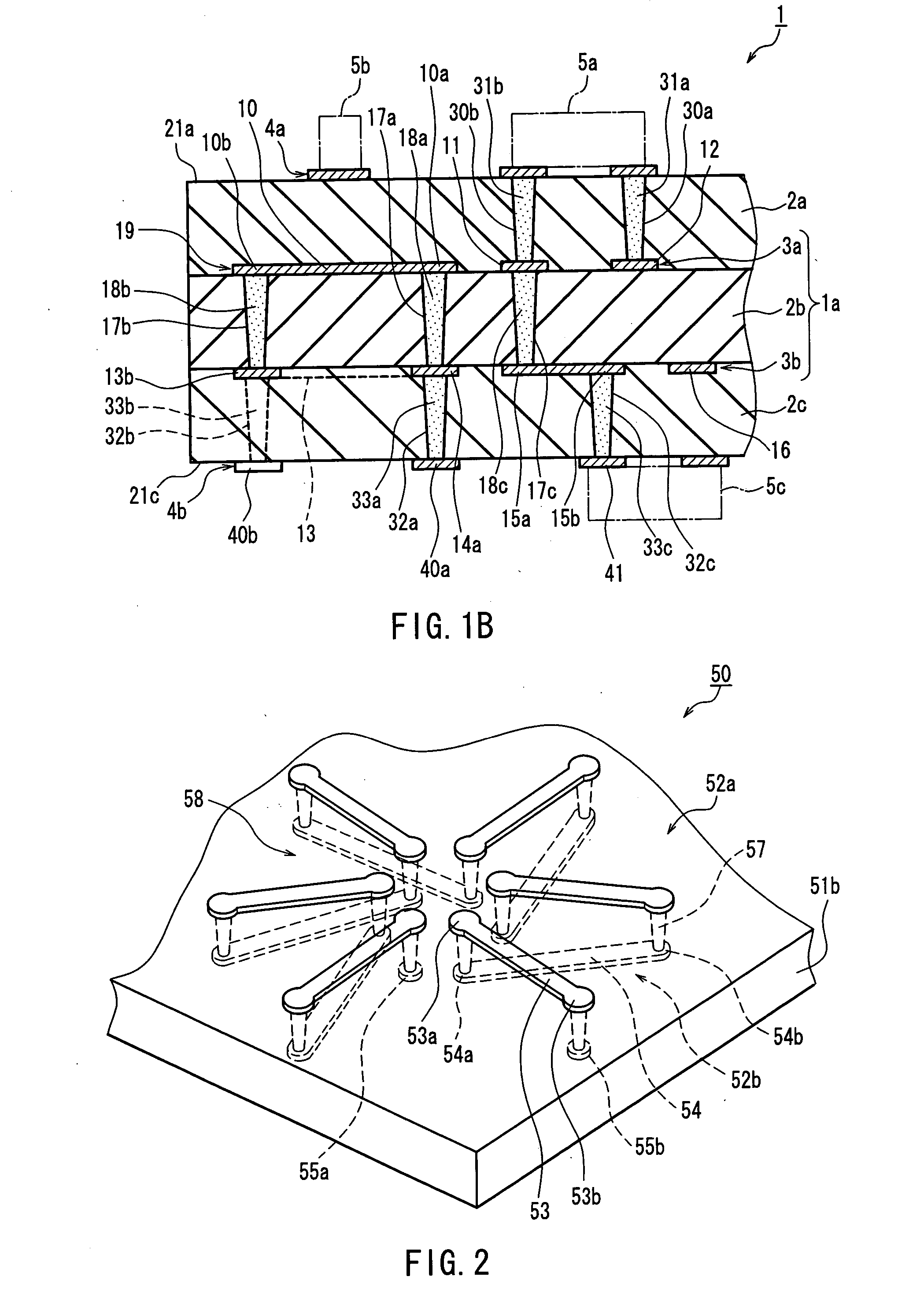
[0043] The following describes Embodiment 2 of the present invention, with reference to the drawings as needed. FIG. 2 to be referred to in the following is a perspective view of a layer provided with a coil in a multilayer circuit board according to Embodiment 2 of the present invention. Since Embodiment 2 is different from Embodiment 1 only in the outside shape of the coil, the following describes such a difference only.

[0044] As shown in FIG. 2, a multilayer circuit board 50 according to Embodiment 2 of the present invention includes: conductive patterned layers 52a and 52b provided on upper and lower surfaces of an electrical insulative base member 51b (corresponding to the electrical insulative base member 2b of Embodiment 1), respectively. Although not illustrated, an electrical insulative base member is provided on the outside of each of the conductive patterned layers 52a and 52b, and a conductive patterned layer further is provided on the outside of each electrical insulat...

embodiment 3

[0047] The following describes Embodiment 3 of the present invention, with reference to the drawings as needed. FIG. 3A to be referred to in the following is a perspective view of a multilayer circuit board according to Embodiment 3 of the present invention, showing each layer separately, and FIG. 3B is a cross-sectional view of the multilayer circuit board according to Embodiment 3 taken along the line II-II of FIG. 3A.

[0048] As shown in FIGS. 3A and 3B, a multilayer circuit board 100 according to Embodiment 3 includes: electrical insulative base members 101a to 101c; conductive patterned layers 102a and 102b provided between the respective electrical insulative base members 101a to 101c; and conductive patterned layers 103a and 103b respectively provided on outer surfaces of 1011a and 101c of the electrical insulative base members 101a and 101c. The multilayer circuit board 100 further includes a first coil 104a formed inside and a second coil 104b formed around this first coil 1...


PUM


Abstract

A multilayer circuit board includes: two or more layers of electrical insulative base members; and two or more layers of conductive patterned layers. At least two of the conductive patterned layers include coil patterns that will be a part of a coil, through holes are provided at predetermined positions of the electrical insulative base members, the positions being sandwiched between the coil patterns, so as to enable communication between respective end portions of the coil patterns, and conductive paste charged in the through holes allows electrical connection to be established between the respective end portions. The coil is formed so as to be wound in a direction perpendicular to a thickness direction of the multilayer circuit board. With this configuration, a multilayer circuit board can be provided, which facilitates increasing the winding number of a coil and has excellent flexibility of circuit design.

Description

FIELD OF THE INVENTION [0001] The present invention relates to a multilayer circuit board including a coil. BACKGROUND OF THE INVENTION [0002] As conventionally known methods for forming a coil, there is a method of forming a plurality of coil patterns, each of which will be a part of a coil, in a circuit board and then connecting these coil patterns electrically so as to form a coil. For instance, as shown in FIG. 9, JP 2001-77538A suggests that coil patterns 402a to 402d shaped like a letter C are formed on principal surfaces of respective layers 401a to 401c of a build-up multilayer board 400, and the coil patterns 402a to 402d are connected via build-up vias 403a to 403c so as to form a circuit board including a patterned coil with a spiral shape as a whole. [0003] Furthermore, as shown in FIG. 10, JP 2000-223316A suggests a circuit board having a coil structure formed as follows: a plurality of coil patterns 501 and 502 are formed to be aligned on upper and lower surfaces 500a ...

Claims


Application Information

Patent Timeline
IPC IPC(8): H05K7/06H05K3/46H01F5/00H01F17/00H05K1/16H05K1/18H05K3/40
CPCH01F17/0013H01F17/0033H05K1/165H05K2201/10416H05K3/4614H05K2201/086H05K2201/097H05K3/4069
Inventor ENCHI, KOUHEIUEDA, YOJI
Owner PANASONIC CORP
Why Eureka
Try Eureka