Coherent DUV illumination for semiconductor wafer inspection

Active Publication Date: 2006-04-20
KLA TENCOR CORP
View PDF8 Cites 10 Cited by
  • Summary
  • Abstract
  • Description
  • Claims
  • Application Information

AI Technical Summary

Benefits of technology

[0011] According to one aspect of the present design, there is provided an apparatus for inspecting a specimen, such as a semiconductor wafer. The apparatus comprises a laser energy source and an optical fiber arrangement. The optical fiber arrangement comprises a core surrounded by a

Problems solved by technology

Previous illuminator designs tend to offer limited brightness levels as measured in terms of watts/cm2-str-nm.
Use of mercury xenon or cascaded arc lamps tends to be limited in that when used with very small sensor pixels and apertured illumination modes, they can be unable to be imaged with sufficient intensity to enable adequate operation of TDI sensors.
Mercury xenon and cascaded arc lamps tend to be limited in the average pow

Method used


Image

  • Coherent DUV illumination for semiconductor wafer inspection
  • Coherent DUV illumination for semiconductor wafer inspection
  • Coherent DUV illumination for semiconductor wafer inspection

Examples


Embodiment Construction

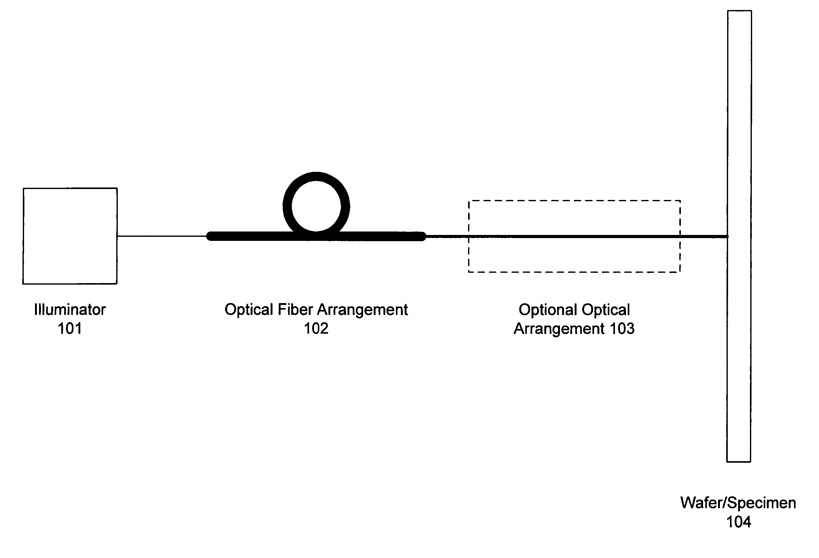
[0020] According to the present invention, there is provided a broadband illuminator transmitting high average power coherent radiation in the range of 150 nm to 500 nm, or portions thereof, for purposes of inspecting a semiconductor wafer. The present design may offer improvements over previously known broadband illumination designs.

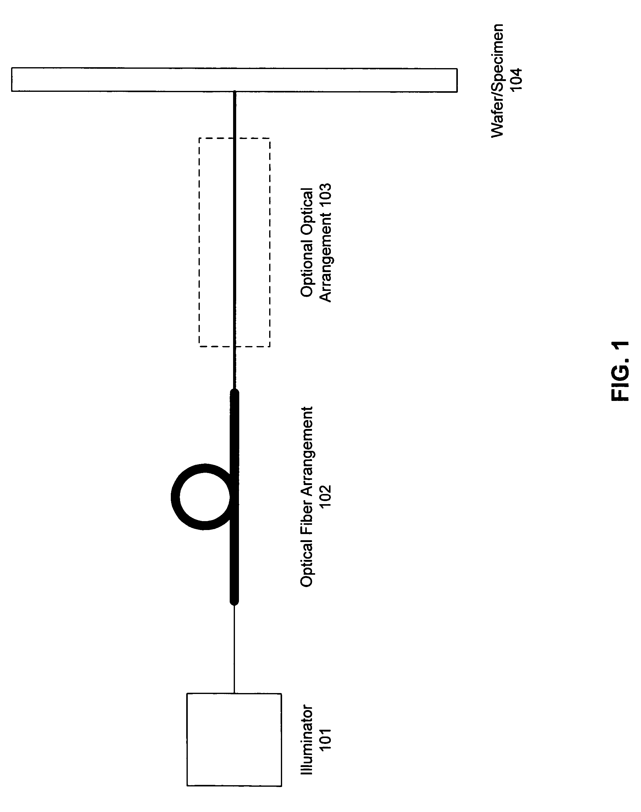
[0021] The present design employs optical fibers to frequency broaden the output of an input laser beam and uses frequency broadened radiation as an illumination source in a brightfield inspection tool. FIG. 1 illustrates a general conceptual arrangement for the present design. From FIG. 1, illuminator 101 may comprise a laser, such as a laser operating in the deep ultraviolet (DUV) range, where the illuminator provides light energy to optical fiber arrangement 102. Light passes through optical fiber arrangement 102 to optional optical arrangement 103 and to the surface of the specimen or semiconductor wafer 104.

[0022] The illuminator 101 may be a mod...


PUM


Abstract

An apparatus for inspecting a specimen, such as a semiconductor wafer, is provided. The apparatus comprises a laser energy source, such as a deep ultraviolet (DUV) energy source and an optical fiber arrangement. The optical fiber arrangement comprises a core surrounded by a plurality of optical fibers structures used to frequency broaden energy received from the laser energy source into frequency broadened radiation. The frequency broadened radiation is employed as an illumination source for inspecting the specimen. In one aspect, the apparatus comprises a central core and a plurality of structures generally surrounding the central core, the plurality of fibers surround a hollow core fiber filled with a gas at high pressure, a tapered photonic fiber, and/or a spider web photonic crystalline fiber, configured to receive light energy and produce frequency broadened radiation for inspecting the specimen.

Description

[0001] This application claims the benefit of U.S. Provisional Patent Application 60 / 620,814, filed Oct. 20, 2004, and entitled “Coherent DUV Sources for Semiconductor Wafer Inspection,” inventors Yung-Ho Chuang, J. Joseph Armstrong, and Richard William Solarz.BACKGROUND OF THE INVENTION [0002] 1. Field of the Invention [0003] The present invention relates generally to the field of illuminators, and more particularly to illuminators employed in the inspection of semiconductor wafers. [0004] 2. Description of the Related Art [0005] Many optical systems provide an ability to inspect or image features on the surface of a specimen, such as inspecting defects on a semiconductor wafer or photomask. Certain advanced semiconductor defect inspection systems can detect defects on the order of 30 nm in size during a full inspection of a 300 mm diameter wafer. [0006] The demands of the semiconductor industry for wafer and photomask inspection systems exhibiting high throughput and improvements ...

Claims


Application Information

Patent Timeline
IPC IPC(8): G02B6/032
CPCG01N21/8806G01N21/9501G02B6/02328G02B6/02357H01S3/302
Inventor SOLARZ, RICHARD WILLIAM
Owner KLA TENCOR CORP
Why Eureka
Try Eureka