Communication device and package thereof

a communication device and a technology of a communication device, applied in the direction of printed circuit non-printed electric components, semiconductor/solid-state device details, instruments, etc., can solve the problems of difficult application of screen printing technology, and achieve the effects of preventing the disconnection of wires, reducing the possibility of damage, and keeping the electrical connection in a nice condition

Inactive Publication Date: 2006-04-27
K UBIQUE ID CORP
View PDF2 Cites 11 Cited by
  • Summary
  • Abstract
  • Description
  • Claims
  • Application Information

AI Technical Summary

Benefits of technology

[0017] Adoption of the fixing means with the molding technology is suitable because the mold material (normally resin) absorbs impacts on collision to reduce the possibility of damaging the communication device of the present invention. It is also possible to keep the electrical connection in a nice condition at the electrically connected portion. In particular, adoption of the wire bonding technology to the electrical connection can prevent disconnection of the wire that is usually very thin and easily breakable.
[0018] Preferably, the insulation substrate 2 or the surface-mount chip antenna 5 has a recess 6, and the RFID part 1 is disposed in the recess 6. This enable the communication device of the present invention to have an outer shape approximated to a cubical shape. The approximated cubical outer shape is excellent in handling. In particular, it is excellent in handling on mounting by a general-purpose automatic mounting machine. The mounting by the general-purpose automatic mounting machine passes through the steps of adsorbing one surface of a cube, and holding and moving the communication device with the adsorbing force. This is effective to limit a location of the RFID part 1 arranged on the insulation substrate 2 or the surface-mount chip antenna 5 within a certain range (the recessed region). As a result, variations in the characteristics and the shape of the communication device of the present invention can be reduced advantageously.

Problems solved by technology

As a result, application of the screen printing technology may become difficult after mounting other components due to the existence of other components.
This is because the screen may contact with projections in the print surfaces of other components to prevent achievement of excellent printings.

Method used


Image

  • Communication device and package thereof
  • Communication device and package thereof
  • Communication device and package thereof

Examples


Embodiment Construction

[0030] The embodiments of the present invention will now be described.

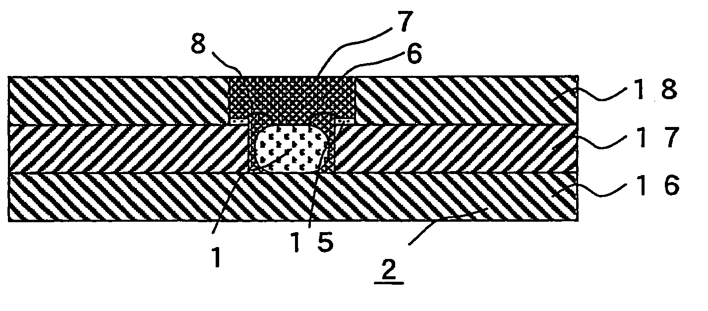
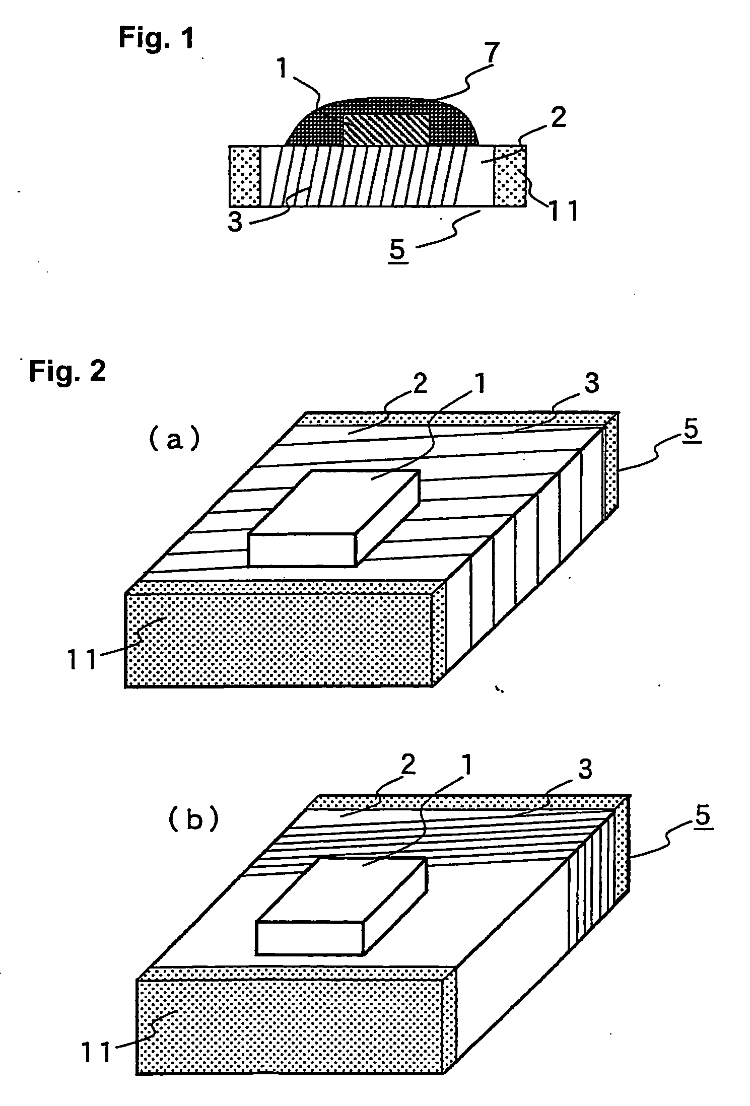
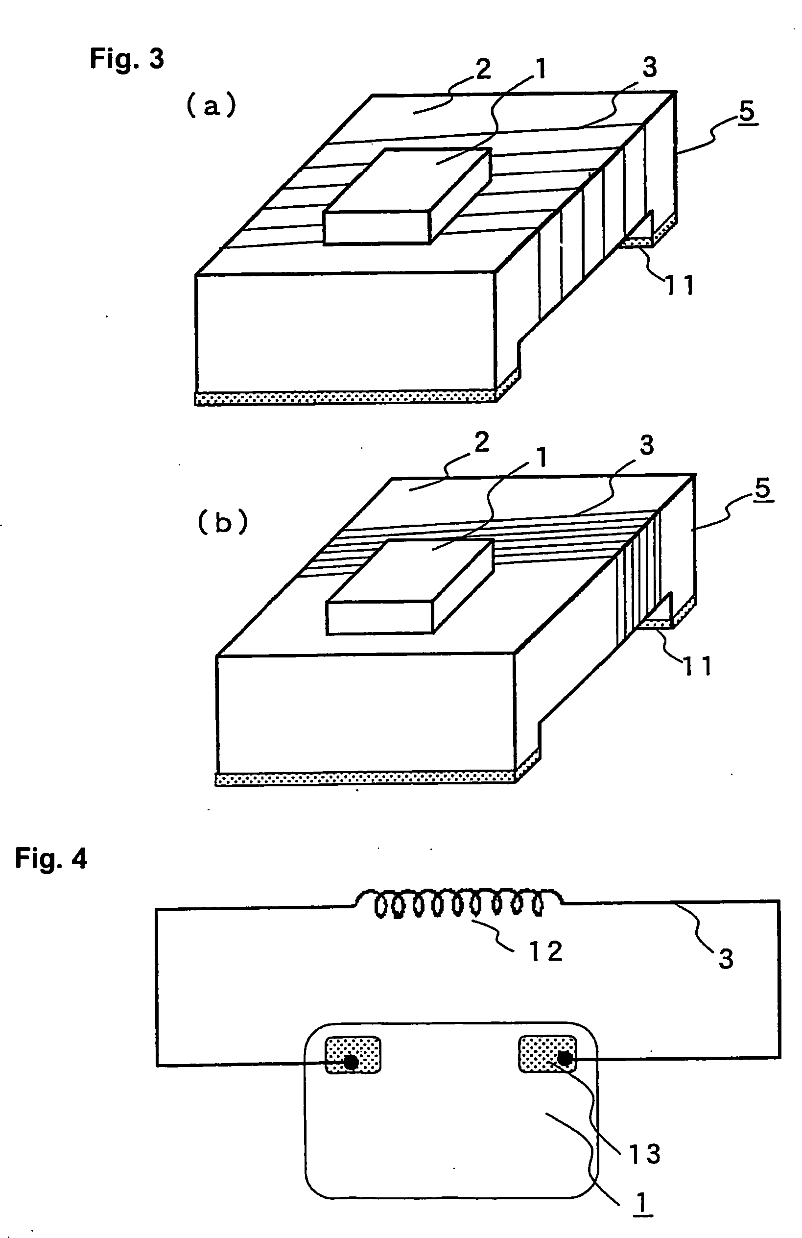
[0031] The RFID part 1 is commercially available. The RFID part 1 is shaped in a chip with outer sizes of about 1 mm width, depth and height each and has antenna terminals 13 provided at two locations. The insulation substrate 2 is a molding of more than 91% pure alumina. The insulation substrate 2 has a sufficient strength so that it can not be broken when sandwiched in the general-purpose mounting machine. It also has a sufficient insulation property.

[0032] In FIG. 2(a), the insulation substrate 2 is shaped in a rectangular solid. The conductive wire 3 is wound around the cover layer of the upper, lower and side faces, that is, the surface of the substrate to configure the chip antenna 5, and the RFID part 1 is mounted thereon. Then, the wire bonding technology is applied to electrically connect the antenna terminal 13 of the RFID part 1 to the conductive wire 3 via a gold wire, not shown. Further, an epoxy re...


PUM


Abstract

A communication device capable of eliminating complexity of mounting a RFID part onto a commodity such as an electronic device. For this, the RFID part is fixed on an insulation substrate and the insulation substrate can be mounted on the surface of a circuit plate. Thus, the RFID part can be mounted onto a commodity by the technique of mounting on the general-purpose circuit plate. This significantly reduces the mounting work and achieves the object of the invention. The communication device may be such that the RFID part is fixed on a surface-mounted chip antenna and the RFID part has an antenna terminal electrically connected to a terminal of the surface-mounted chip antenna.

Description

TECHNICAL FIELD [0001] The present invention relates to a communication device and package thereof. The communication device uses a RFID part and is particularly placed on an electronic device. BACKGROUND ART [0002] In recent years, product development and consideration have been proceeded for the communication device that uses a RFID (Radio Frequency Identification) technology. Such the communication device is capable of serving as an alternative to conventional bar codes, containing (storing) a large amount of information, easy and relatively distant information reading in non-contact with an information reader named scanner, and writing information into the RFID part. Accordingly, its applications to various uses are expected. [0003] The above uses include its attachment to a courier parcel to easily trace the parcel delivery, and individual management of massive various commodities in music CD stores and bookstores. The attachment is usually achieved by sticking a resinous film ...

Claims


Application Information

Patent Timeline
Patent Type & Authority Applications(United States)
IPC IPC(8): G06K19/06G06K19/04G06K19/077H01L23/498H01Q1/22H01Q1/24H01Q1/38H01Q7/00H01Q7/08H05K1/18
CPCG06K19/041G06K19/07749G06K19/0775G06K19/07758G06K19/07779G06K19/07781H01L23/49855H01L2224/16H01L2924/01079H01Q1/22H01Q1/2225H01Q1/24H01Q1/38H01Q7/00H01Q7/08H05K1/181H01L2224/45144
Inventor TAKAYAMA, TOSHIHARU
Owner K UBIQUE ID CORP
Why Eureka
Try Eureka