Method for molding a small form factor digital memory card

Active Publication Date: 2006-12-14
KINGSTON DIGITAL CO LTD
View PDF4 Cites 39 Cited by
  • Summary
  • Abstract
  • Description
  • Claims
  • Application Information

AI Technical Summary

Benefits of technology

[0016] Runner gate openings at which to inject the resin mold material from respective runner gates into the mold cavity to encapsulate the PCA subassembly are preferably located above the rows of external leads along opposite sides of the TSOP flashcard package. In addition, a runner gate opening may be located above the front edge of the flashcard package. Thus, resin will flow downwardly from an overhead location to first cover the leads and then the top of the flashcard package. By virtue of the top down resin flow pattern, the lateral shear forces and the bending forces to be applied to the TSOP flashcard package during molding will be reduced so as to correspondingly reduce the possibility of damaging the delicate flash IC that is inside the flash

Problems solved by technology

However, the ICs are not assembled in a package as would otherwise occur in the aforementioned SMT production line assembly process.
Nevertheless, when using the COB process, the supporting passive components may still need to be surface mounted to the substrate by means of an SMT assembly line.
The desirable injection molded method has not typically been applicable to PCAs that are made from the IC package/SMT process.
This leaves very little room for injection molding in areas directly above the TSOP package.
Therefore, a PCA containing relatively tall packages, like the standard TSOP package, is unsuitable for injection molding.
Although the injection mold process to form an integral cover for the final memory card assembl

Method used


Image

  • Method for molding a small form factor digital memory card
  • Method for molding a small form factor digital memory card
  • Method for molding a small form factor digital memory card

Examples


Example

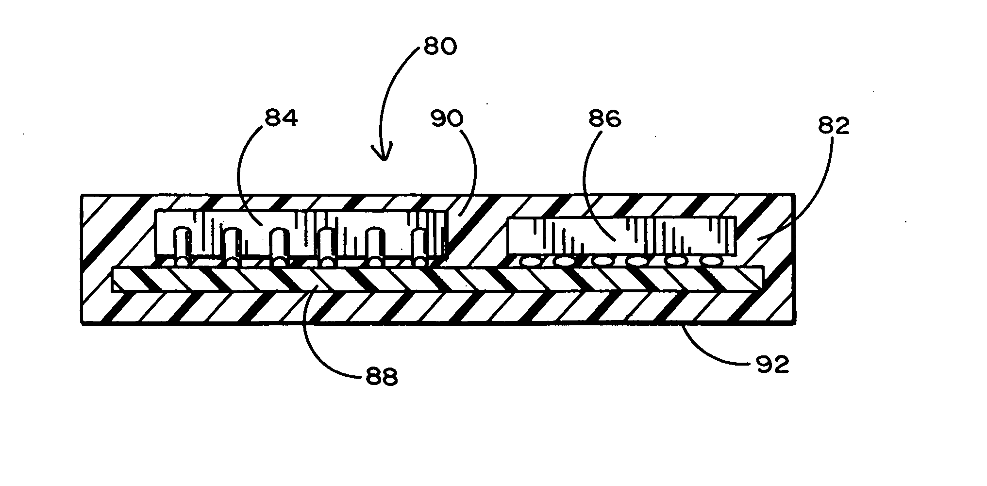
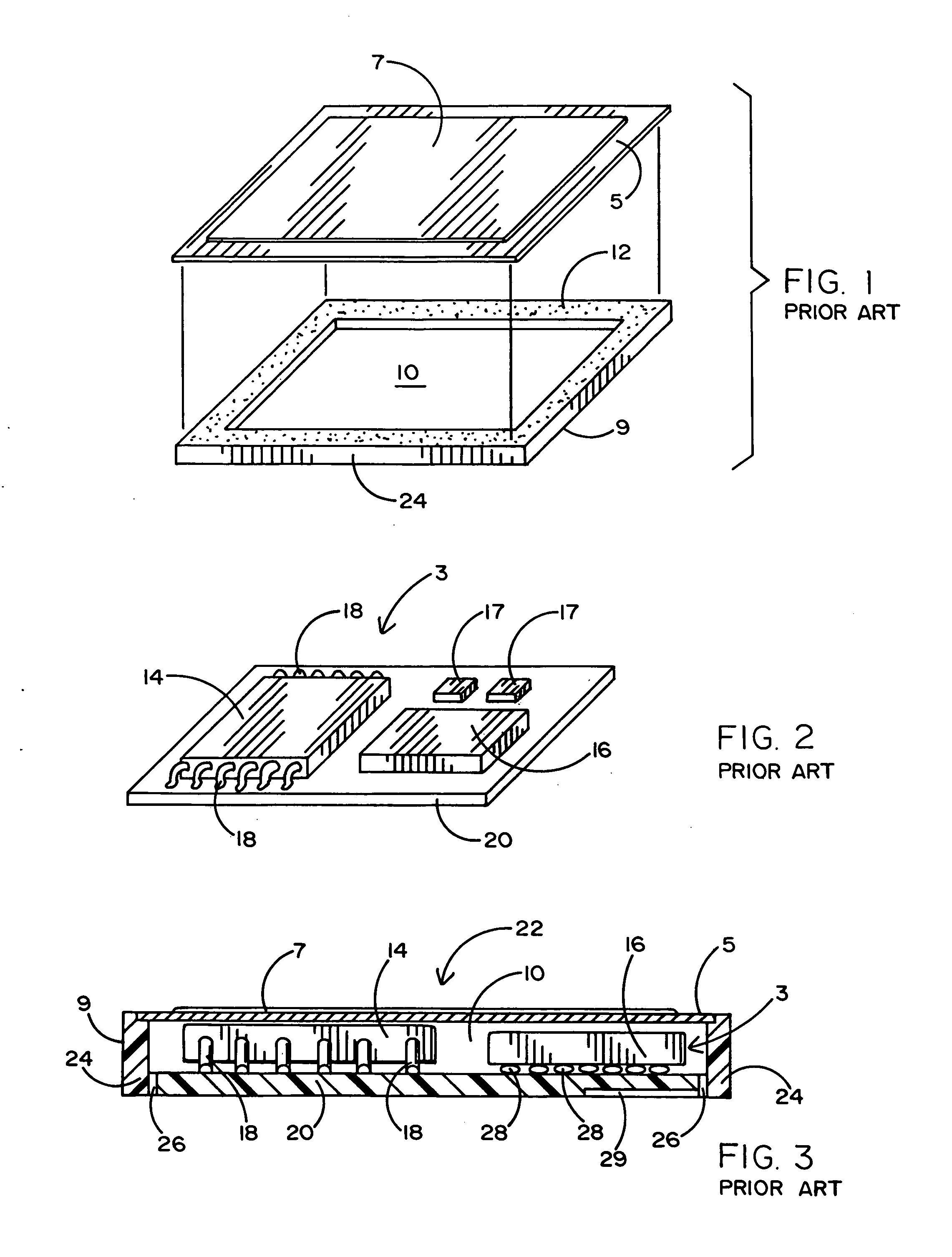
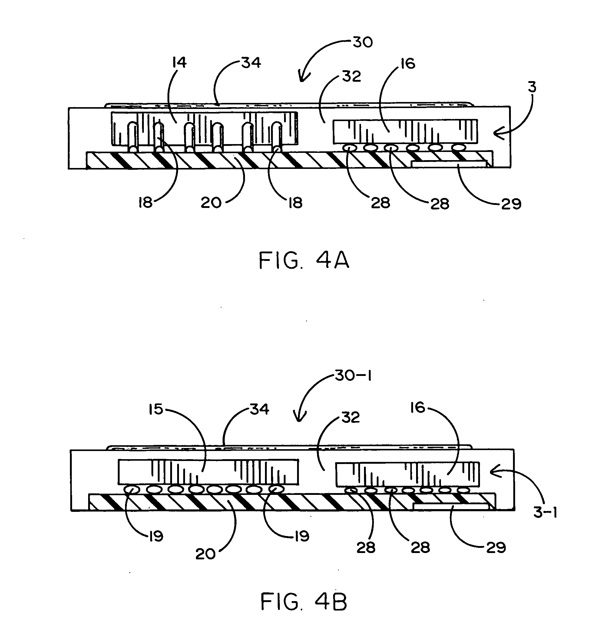
[0029]FIG. 1 of the drawings shows a conventional case subassembly 1 to surround and cover a PCA subassembly 3 of the kind shown in FIG. 2. The PCA subassembly 3 includes flash and controller packages and conventional passive components mounted on a printed circuit board. FIG. 3 shows the PCA subassembly 3 after it has been located within a hollow cavity 10 of the case subassembly 1. The foregoing is typical of a well-known technique used for manufacturing multimedia cards (MMC).

[0030] In particular, a thin metal foil cover 5 of the case subassembly 1 having a label sheet 7 affixed thereto is connected overtop a plastic frame 9 having the hollow cavity 10 located therewithin. The thin metal foil cover 5 is used as a top for the frame 9 so as to provide a sufficient space (of about 0.10 mm or less) above the PCA subassembly 3 (best shown in FIG. 3) while maintaining a desired overall card thickness of approximately 1.40 mm to meet MMC industry standards. Although it would be possibl...


PUM

PropertyMeasurementUnit
Flow rateaaaaaaaaaa
Plasticityaaaaaaaaaa

Abstract

A method for molding digital storage memory cards such as, for example, multimedia cards (MMC), secure digital cards (SD), and similar small form factor digital memory cards. A PCA subassembly including, for example, a leadframe (TSOP) package for enclosing a flash IC and a (e.g., land grad array) controller package for enclosing a controller IC are mounted on a printed wiring board within a mold cavity. A high melt flow index resin is injected into the mold cavity to form an integral, solid body within which to completely encapsulate the flash IC and controller packages and form a cover over top the flash IC package so as to maintain the required memory card height tolerance. In one embodiment, the resin material is injected downwardly into the mold cavity from locations above the respective rows of leads of the flash IC package. In another embodiment, the resin material is injected laterally into the mold body from locations at opposite sides thereof adjacent the respective rows of leads of the flash IC package.

Description

BACKGROUND OF THE INVENTION [0001] 1. Field of the Invention [0002] This invention relates to a method for molding digital storage memory cards such as, for example, multimedia cards (MMC), secure digital cards (SD), and similar small form factor digital memory cards. [0003] 2. Background Art [0004] Thin form factor digital flash memory cards such as secure digital (SD), mini-SD, multimedia cards (MMC), and others contain three major components: an active flash memory device (including a flash IC and its controller); a printed circuit board (PCB) substrate; and an exterior cover that is typically manufactured from plastic. There are commonly two conventional methods of making these thin form factor digital memory cards. [0005] The first method requires that semiconductor packages are surface mounted on the PCB substrate by way of a SMT production line. In this case, the active components (i.e., the flash memory and controller ICs) are located inside the semiconductor packages. These...

Claims


Application Information

Patent Timeline
IPC IPC(8): H01L21/00
CPCB29C45/14647B29C45/14655H01L2924/0002B29C45/14836B29C45/2708H01L21/565H05K1/117H05K3/284H05K2201/10159H05K2201/10689H05K2201/10734H05K2203/1311H05K2203/1316H05K2203/304H01L2924/00
Inventor KOH, WEI H.CHEN, BEN W.CHEN, DAVID H. D.
Owner KINGSTON DIGITAL CO LTD
Why Eureka
Try Eureka