Ubm structure for improving reliability and performance

Inactive Publication Date: 2006-04-27
TAIWAN SEMICON MFG CO LTD
View PDF59 Cites 20 Cited by
  • Summary
  • Abstract
  • Description
  • Claims
  • Application Information

AI Technical Summary

Benefits of technology

[0009] A novel UBM structure for improving the reliability and performance of the UBM structure and associated device is described. The UBM structure comprises a plurality of metallic layers, which are deposited onto an electrically conductive element, such as a bonding pad of a semiconductor device. The UBM structure is provided as an interface between the bonding pad and another electrically conductive element, such as solder material deposited over the UBM structure. In one embodiment, the UBM structure includes layers of nickel and copper in which nickel is the upper layer in contact with the solder material. The nickel layer is formed to include a downwardly depending perimeter portion, which serves as a cover to the copper layer of the UBM structure. Accordingly, the copper layer is shielded from contact with the solder material during a reflow process, thereby avoiding undesirable rea

Problems solved by technology

Solder bumps, however, are generally not applied directly to the bonding pads of the semiconductor wafer.
It has been found that the direct application of solder bump material to the semiconductor wafer yields poor electrical conduction, due largely to the rapid oxidation of the final metal layer (e.g. aluminum) upon exposure to air.
Moreover, aluminum has been found to be neither particularly wettable nor bondable with most solders.
It has been found that prior art UBM structures tend to experience poor reliability and performance when solder material comes in contact with copper of the UBM structure during the solder bump formation process.
These reactions ar

Method used


Image

  • Ubm structure for improving reliability and performance
  • Ubm structure for improving reliability and performance
  • Ubm structure for improving reliability and performance

Examples


Embodiment Construction

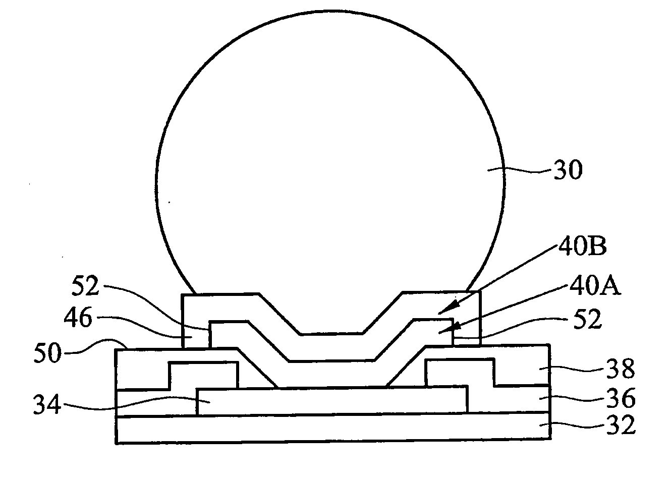
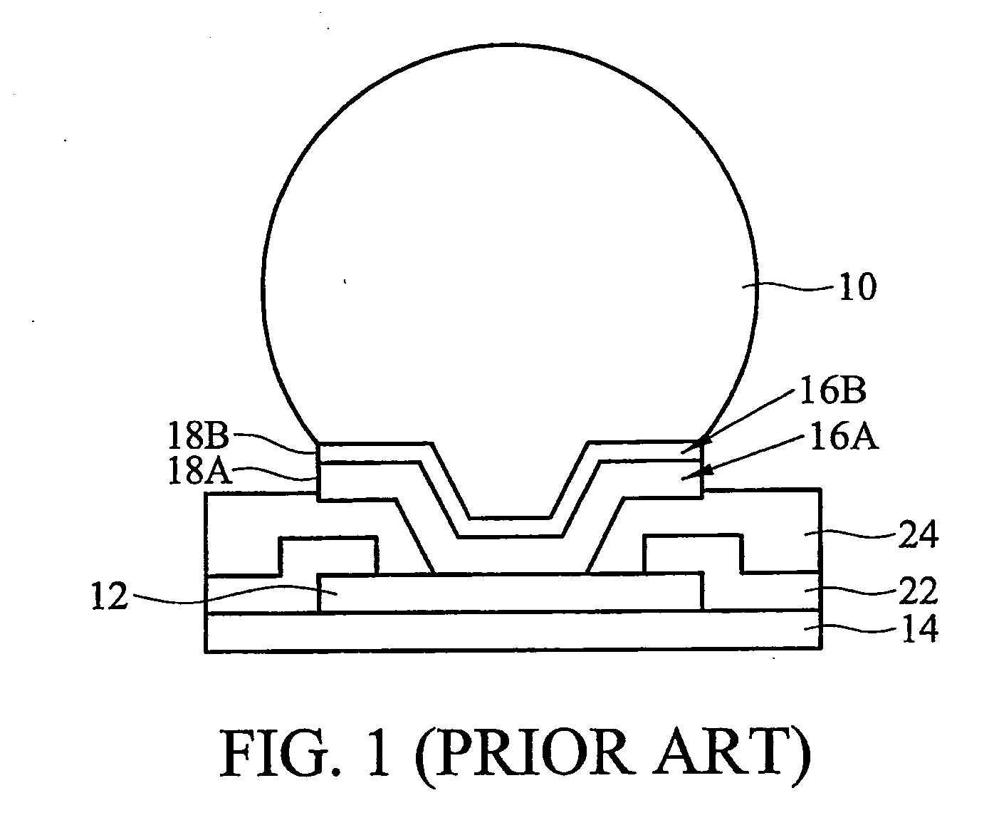
[0015] UBM structures may be utilized in any arrangement requiring bonding between electrically conductive components. By way of example, UBM structures are often utilized in the manufacture of semiconductor devices. Although this disclosure describes unique UBM structures in the context of implementation into semiconductor devices, it is contemplated that the UBM structures of the present disclosure may be incorporated into devices other than semiconductor devices.

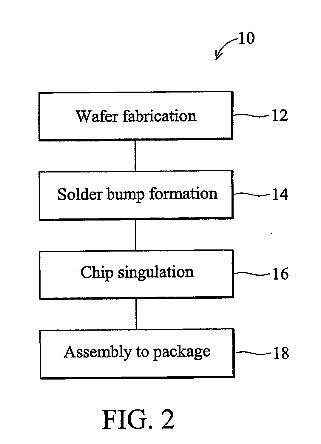
[0016]FIG. 2 is a block diagram illustrating an exemplary semiconductor manufacturing process 10 associated with producing chips for use in semiconductor applications. The process 10 includes wafer fabrication 12, which generally involves layering, patterning, doping, and applying heat treatments to a silicon wafer. The process 10 further includes forming solder bumps 14 on the fabricated wafer. The solder bumps generally facilitate electrical and mechanical connection between chip devices singulated from the fabricated ...


PUM


Abstract

A novel under-bump metallization (UBM) structure for providing electrical communication is described. The UBM structure includes a plurality of metallic layers, which are deposited onto a bonding pad of a semiconductor device, such as a semiconductor chip. The UBM structure may be provided as an interface between the bonding pad and a solder bump deposited over the UBM structure. In one example, the UBM structure includes layers of nickel and copper in which nickel is the upper layer in contact with the solder bump and copper is the lower layer in contact with the bonding pad. The nickel layer is formed to include a downwardly depending perimeter portion, which serves as a cover to the copper layer of the UBM structure. Accordingly, the copper layer is shielded from contact with the solder material during the reflow process, thereby avoiding undesirable reactions between the copper and solder.

Description

TECHNICAL FIELD [0001] Disclosed embodiments herein relate generally to semiconductor wafer processing, and more particularly to improved under-bump metallization (UBM) structures and associated methods for improving reliability and performance of such UBM structures. BACKGROUND [0002] UBM structures are often utilized during semiconductor manufacturing processes. Semiconductor manufacturing processes generally begin with processes associated with fabricating a semiconductor wafer such as layering, patterning, doping, and heat treatments. Once fabricated, semiconductor wafers undergo additional processes associated with testing, packaging, and assembling semiconductor IC chips obtained from the wafers. Semiconductor manufacturing processes are continually being refined, modified, and improved in light of breakthroughs in semiconductor technology. One such technology that has continued to gain increased acceptance is “flip chip” technology, which refers to microelectronic assemblies ...

Claims


Application Information

Patent Timeline
IPC IPC(8): H01L23/48H01L21/44
CPCH01L24/11H01L2224/1147H01L2924/0002H01L2224/0401H01L2224/05562H01L2224/05558H01L2224/05572H01L2224/11902H01L2224/131H01L2924/01013H01L2924/01015H01L2924/01022H01L2924/01029H01L2924/01082H01L2924/01322H01L2924/01327H01L2924/14H01L2924/3025H01L24/13H01L2924/00013H01L2924/01005H01L2924/01006H01L2924/01033H01L2924/014H01L2224/05027H01L2224/13099H01L2224/05552H01L2224/05124H01L2224/05147H01L2224/05655H01L2224/11502H01L2224/11849H01L2224/11462H01L24/03H01L24/05H01L2924/00014
Inventor CHENG, CHIU SUNGCHEN, SHIH-MINGYU, H.M.LIN, KUO-WEITSENG, LI-HSIN
Owner TAIWAN SEMICON MFG CO LTD
Why Eureka
Try Eureka