Semiconductor device and its manufacturing method

a manufacturing method and semiconductor technology, applied in semiconductor devices, semiconductor/solid-state device details, electrical equipment, etc., can solve the problem of one physical limit, called fine-line

Inactive Publication Date: 2006-05-04
KK TOSHIBA
View PDF8 Cites 84 Cited by
  • Summary
  • Abstract
  • Description
  • Claims
  • Application Information

AI Technical Summary

Benefits of technology

[0015]FIGS. 4A, 4B are diagrams showing an example of the manufacturing process of the semiconductor memory device of the first embodiment sequent to that of FIGS. 3A, 3B: FIG. 4A is a sectional view of a trench vertical to a longitudinal direction, and FIG. 4B is a sectional view parallel to the silicon substrate surface cut near a center of a trench depth shown along a cutting line 4B-4B of FIG. 4A;
[0016]FIGS. 5A to 5C are diagrams showing an example of the manufacturing process of the semiconductor memory device of the first embodiment sequent to that of FIGS. 4A, 4B: FIG. 5A is a sectional view of a trench vertical to a longitudinal direction, FIG. 5B is a sectional view parallel to the silicon substrate surface cut near a center of a trench depth along the cutting line 5B-5B of FIG. 5A, and FIG. 5C is a sectional view of a side face of the trench in the longitudinal direction along a cutting line 5C-5C of FIG. 5A;
[0017]FIGS. 6A, 6B are diagrams showing an example of the manufacturing process of the semiconductor memory device of the first embodiment sequent to that of FIGS. 5A to 5C: FIG. 6A is a sectional view of a trench vertical to a longitudinal direction, and FIG. 6B is a sectional view parallel to the silicon substrate surface cut near a center of a trench depth shown along a cutting line 6B-6B of FIG. 6A;
[0018]FIGS. 7A, 7B are diagrams showing an example of the m...

Problems solved by technology

However, when miniaturization is further pursued, there is one physical limit, called as a fine-line effect.
This structure is not applicable to a semiconductor device with a feature size of 20 nm or less because it is hard to reduce a trench size to such an extent without causing the fine-line effect.
In a...

Method used


Image

  • Semiconductor device and its manufacturing method
  • Semiconductor device and its manufacturing method
  • Semiconductor device and its manufacturing method

Examples


first embodiment

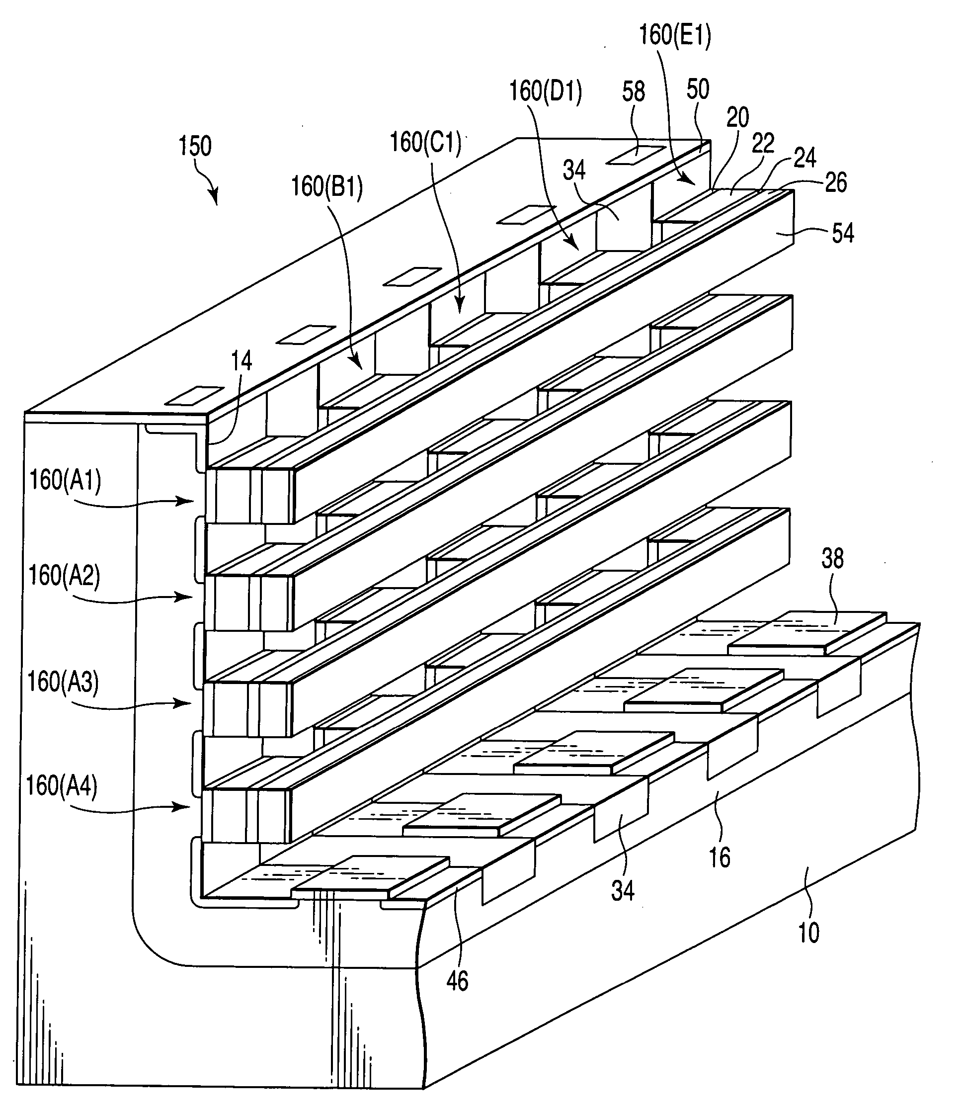
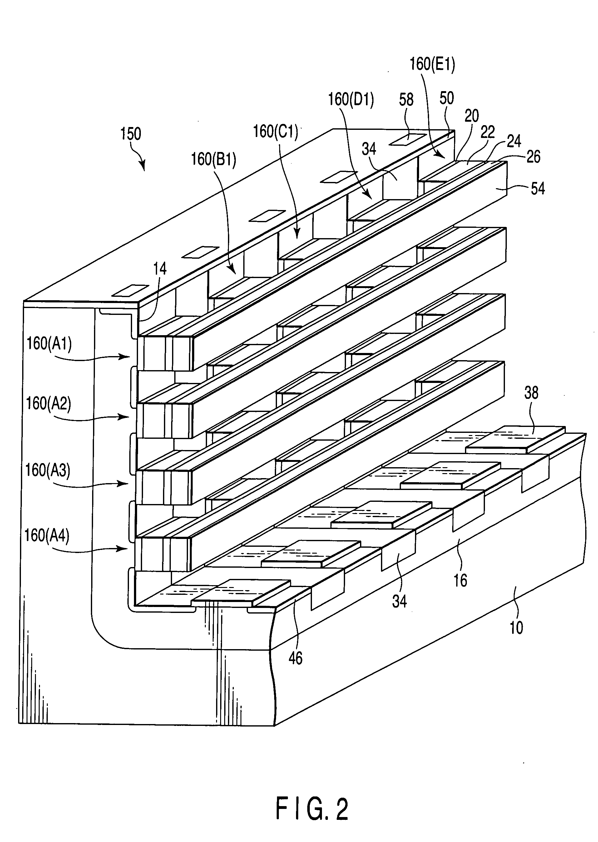
[0037] A first embodiment of the present invention is directed to a three-dimensional semiconductor memory device in which a plurality of thin and long trenches are formed in a semiconductor substrate, and two-dimensionally arranged functional elements such as NAND type memory cells are formed on side faces of both sides.

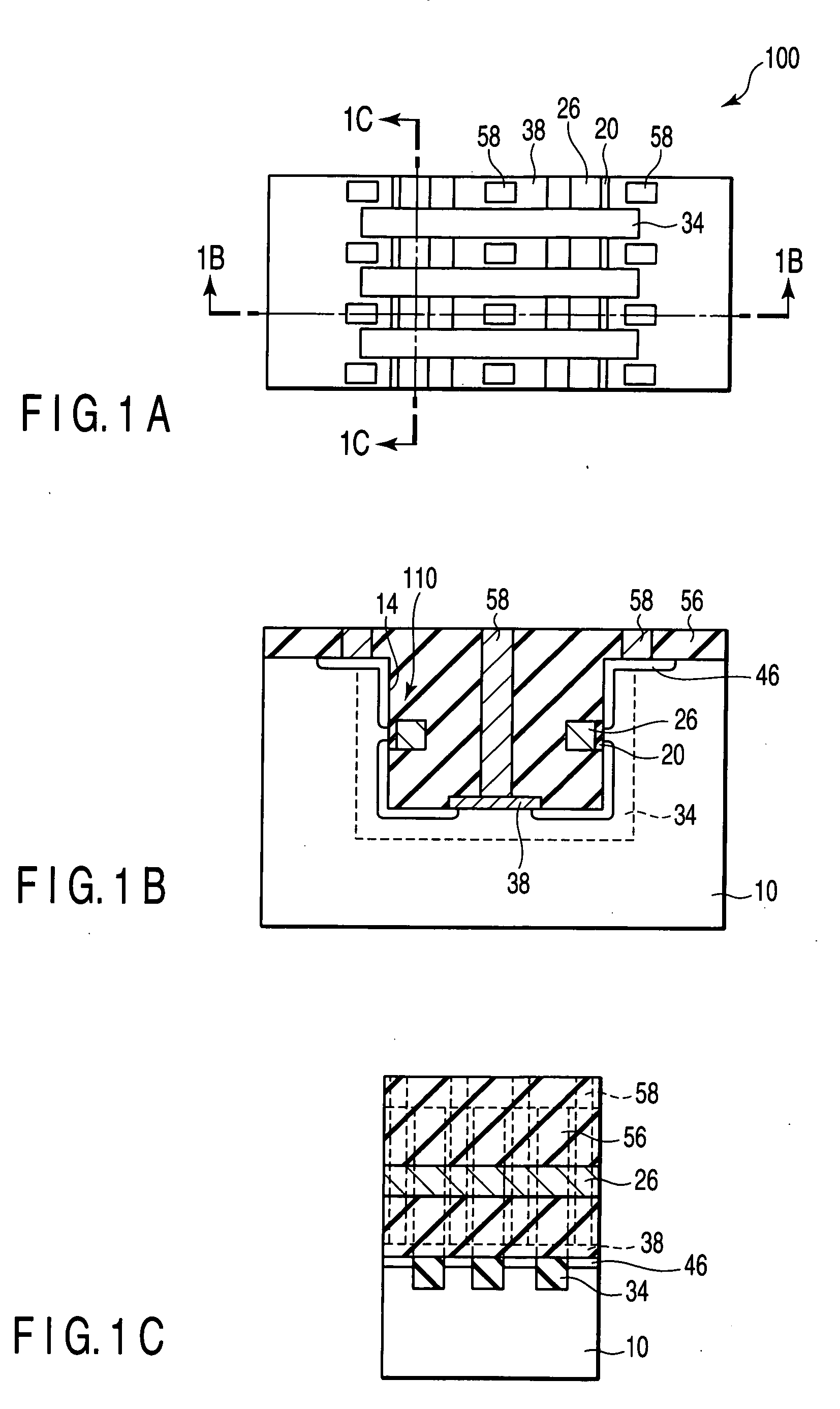
[0038]FIG. 2 is a perspective diagram illustrating a three-dimensional semiconductor memory device 150 according to the embodiment. The embodiment is a NAND type memory cell array 150 formed by arranging two-dimensional memory cells 160 on a side face of a trench 14. In the drawing, parts are omitted to help to understand a structure of the three-dimensional semiconductor memory device 150. Each memory cell 160 includes a gate insulator 20, a floating gate electrode (FG) 22, an interelectrode insulator 24, and a control gate electrode (CG) 26. The FG's 22 of the memory cells 160 such as memory cells 160(A1) to 160(E1) formed in a horizontal direction of the trench ...

second embodiment

[0090] A second embodiment is a method of processing a side face of a concave portion, such as a trench, in a direction parallel to a bottom face. The embodiment will be described by taking an example in which a trench is formed in a semiconductor substrate or a semiconductor layer and a side face of the trench is processed in a direction parallel to the bottom face, as in the case of the step (6) of the first embodiment. However, the embodiment is not limited to this example. By way of example, a manufacturing process of the embodiment will be described RIE etching with reference to FIGS. 12A, 12B to FIGS. 17A, 17B, and 17C.

[0091] (1) FIG. 12A is a sectional view of the trench 14 vertical to a longitudinal direction showing a film 60 to be processed and a mask insulator 62 are formed on the side face of the trench 14 formed in the silicon substrate 10 by a method, for example, similar to that of the aforementioned steps (5) and (6) of the first embodiment or the like. FIG. 12B is ...

third embodiment

[0106] A third embodiment is directed to a structure of a contact connected to a plurality of wirings formed on a side face a trench and arranged in a vertical direction to be parallel to a bottom face of the trench 14 as in the case of the CG's 26 of the first embodiment, i.e., word lines 26, and its manufacturing method.

[0107]FIG. 18 is a diagram showing a structure of a three-dimensional wiring contact 300 which is an example of the embodiment. FIG. 18 shows a side face of the trench 14 near an end thereof. According to the embodiment, a plurality of contact plugs 70n to 701 are formed to connect corresponding wirings 26n to 261. Positions of the wiring contact plugs 701 to 70n on a surface are changed with respect to depths of the corresponding wirings 261 to 26n. A contact plug 70n correspond to the deepest wiring 26n is positioned closest to an end of the trench, and the larger a distance between the contact plug 70 and the end of the trench, the shallower the wiring 26 becom...


PUM


Abstract

A semiconductor device with a new three-dimensional structure comprises a semiconductor substrate including a trench vertically formed to a surface of the semiconductor substrate, a plurality of isolations formed in side and bottom surfaces of the trench in a depth direction of the trench, a plurality of functional elements formed on the side surfaces of the trench separated be the isolation and including an insulator, an electrode formed on the insulator and a pair of source/drain formed in the both sides of the electrode in the depth direction, and a wiring connected to the electrodes located in both sides of the isolation.

Description

CROSS-REFERENCE TO RELATED APPLICATIONS [0001] This application is based upon and claims the benefit of priority from prior Japanese Patent Application No. 2004-314328, filed Oct. 28, 2004, the entire contents of which are incorporated herein by reference. BACKGROUND OF THE INVENTION [0002] 1. Field of the Invention [0003] The present invention relates to a semiconductor device and its manufacturing method, and more particularly to a highly integrated three-dimensional semiconductor device and its manufacturing method. [0004] 2. Description of the Related Art [0005] For an integrated circuit, high integration has been achieved by miniaturizing elements which constitute the circuit. However, when miniaturization is further pursued, there is one physical limit, called as a fine-line effect. The fine-line effect is a phenomenon, for example, resistance of a metal increases exponentially if a size of the metal wiring becomes 20 nm or less. If a wiring width becomes 20 nm or less, the re...

Claims


Application Information

Patent Timeline
IPC IPC(8): H01L23/48
CPCH01L21/8221H01L27/0688H01L27/11551H01L27/11556H01L27/1052H10B99/00H10B41/20H10B41/27
Inventor SHIGEOKA, TAKASHI
Owner KK TOSHIBA
Why Eureka
Try Eureka