Plasma display panel

Inactive Publication Date: 2006-05-04
SAMSUNG SDI CO LTD
View PDF14 Cites 1 Cited by
  • Summary
  • Abstract
  • Description
  • Claims
  • Application Information

AI Technical Summary

Benefits of technology

[0010] It is also an object of the present invention to provide a design for a PDP that allows for more phosphor to be deposited in the discharge cells.
[0011] It is further an object of the present invention to provide a design for a PDP that produces a efficient discharge that can be uniformly transferred to the p

Problems solved by technology

In spite of increased luminous efficiency, the facing discharge-type PDP has a disadvantage in that a phosphor layer is easily deteriorated by plasma.
However, surface discharge AC PDPs have limited performance because of their design.
For example, the shape of the discharge cells li

Method used


Image

  • Plasma display panel
  • Plasma display panel
  • Plasma display panel

Examples


first embodiment

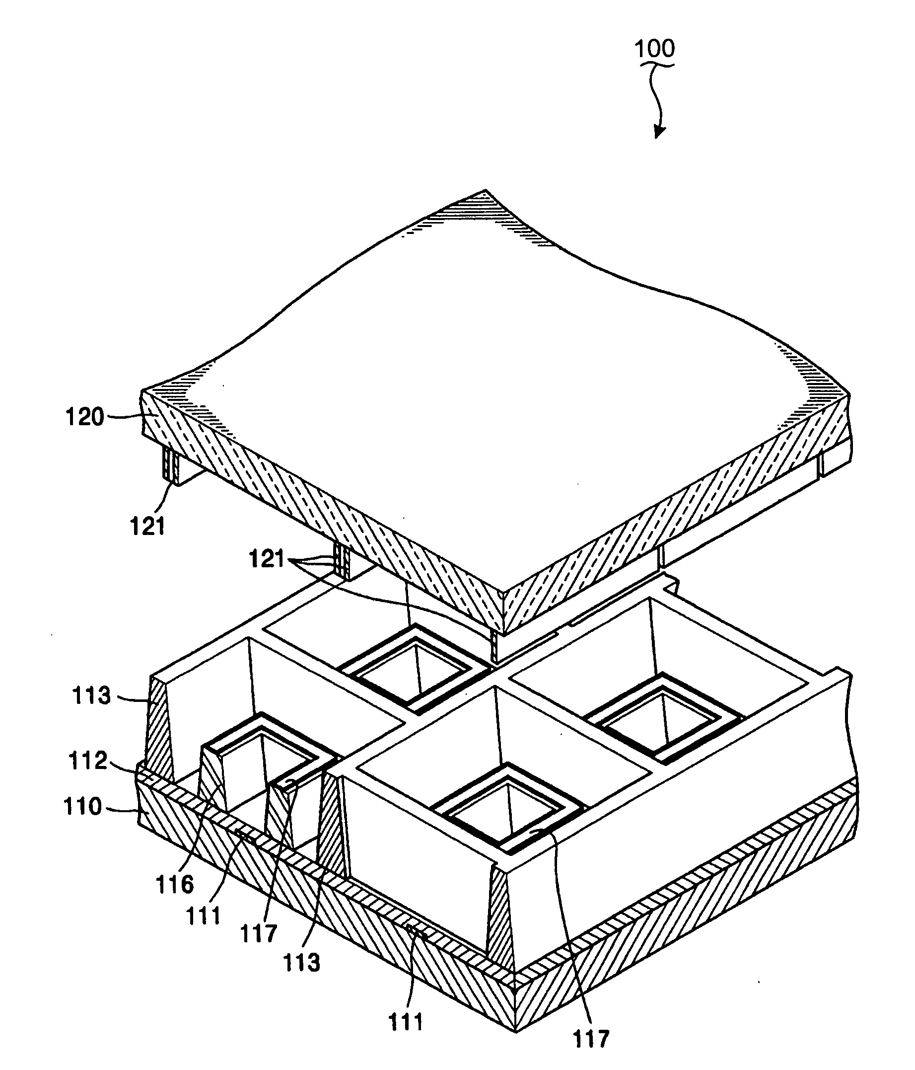
[0038] Turning now to FIGS. 3 through 5, FIG. 3 is an exploded perspective view of a PDP 100 according to the present invention, FIG. 4 is a cross-sectional view of the PDP 100 of FIG. 3 and FIG. 5 is a perspective view depicting electrodes employed in the PDP 100 of FIG. 3. For the sake of clarity, a second dielectric layer 123, a phosphor layer 115, and a line connecting the electrodes are not illustrated in FIG. 3 even though these features are part of the design of PDP 100.

[0039] Referring to FIGS. 3 through 5, a lower substrate 110 and an upper substrate 120 are arranged opposite to each and spaced apart by a certain distance. A discharge space is located between the lower substrate 110 and the upper substrate 120. The lower substrate 110 and the upper substrate 120 are generally made of glass.

[0040] A plurality of address electrodes 111 are located on an upper surface of the lower substrate 110. The address electrodes 111 can have the shape of a band (or stripe) as illustrate...

second embodiment

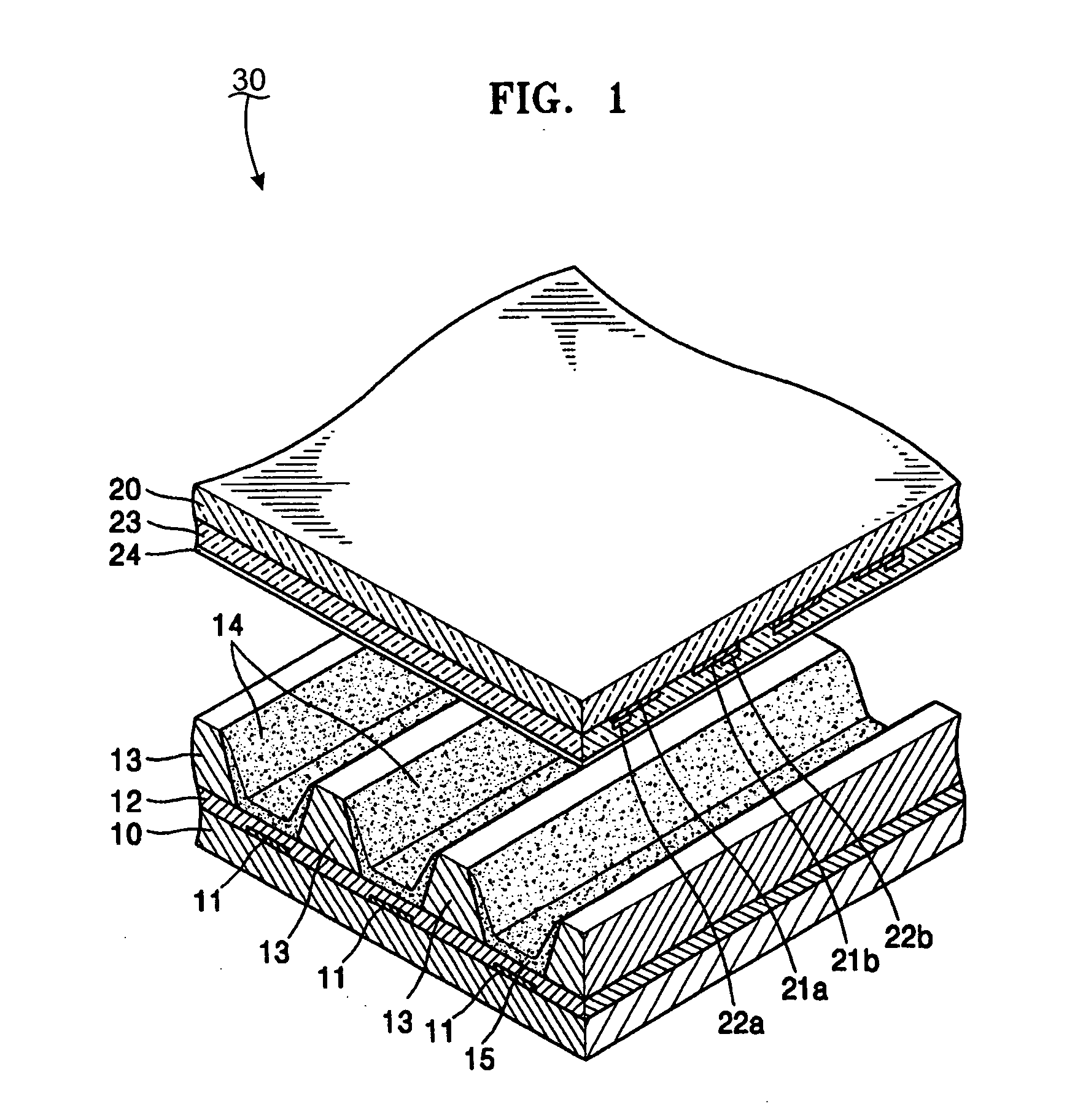
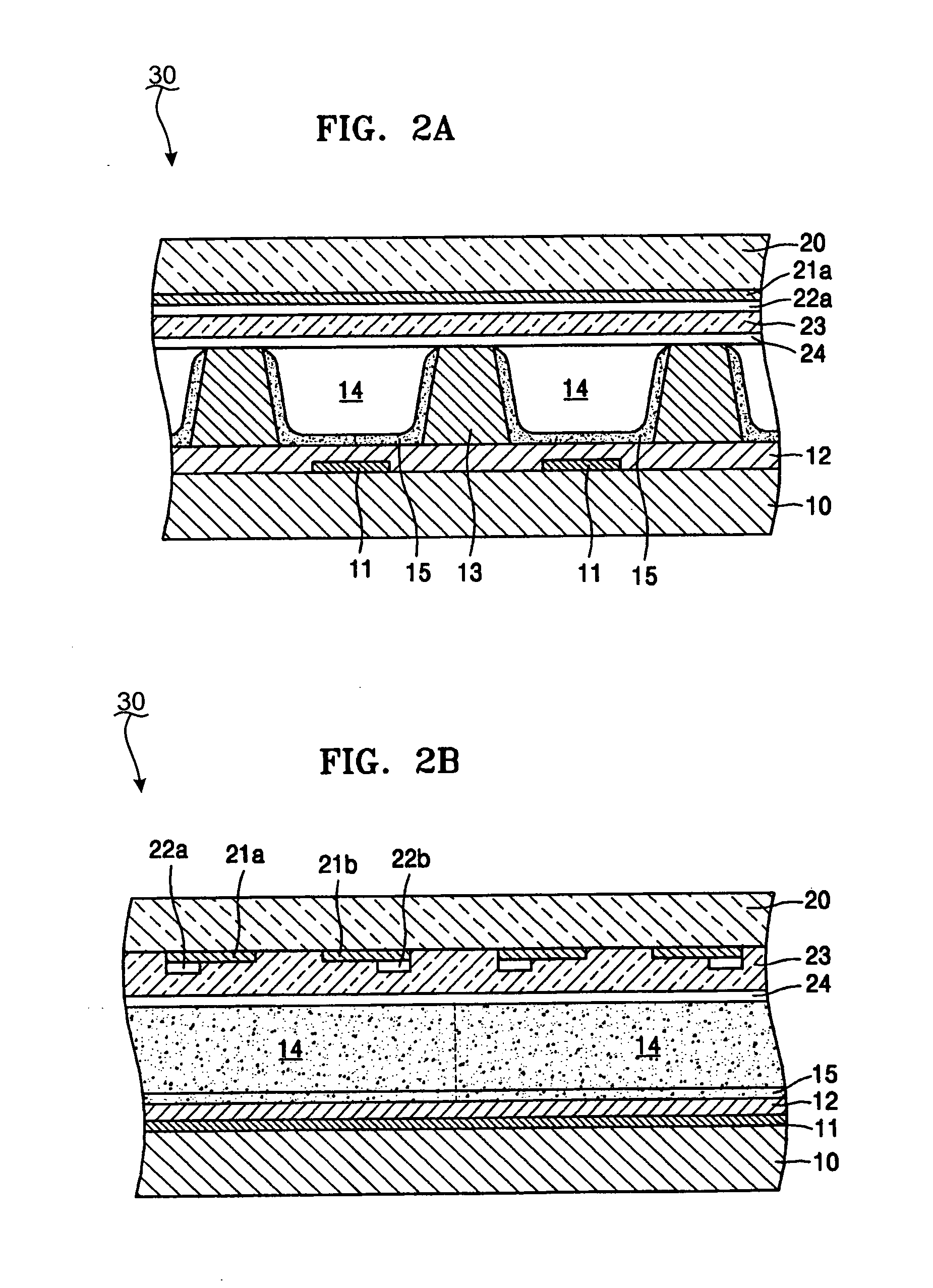
[0053] Turning now to FIGS. 9 through 11, FIGS. 9 through 11 illustrate views of PDP 200 according to the present invention, where FIG. 9 is an exploded view of PDP 200, FIG. 10 is a cross sectional view of PDP 200 and FIG. 11 is a perspective view of the electrodes used in PDP 200 of FIGS. 9 and 10.

[0054] Referring to FIGS. 9 through 11, a lower substrate 210 and an upper substrate 220 are arranged opposite to each other and separated from each other by a certain distance. A discharge space is located between the lower substrate 210 and the upper substrate 220. A plurality of address electrodes 211 are located on an upper surface of the lower substrate 210, and a first dielectric layer 212 is formed over the address electrodes 211 to cover the address electrodes 211. The address electrodes 211 can have the shape of a band, as illustrated of FIG. 11. Alternatively, an address electrode 211′ can have a rectangular plate shape having an aperture located at the center thereof, as illus...


PUM


Abstract

A plasma display that includes a lower substrate and an upper substrate arranged opposite to each other and separated by a constant distance, with a discharge space being arranged between the substrates, a plurality of partitions arranged between the lower substrate and the upper substrate that partition the discharge space into a plurality of discharge cells, a plurality of address electrodes arranged on an upper surface of the lower substrate, a first dielectric layer arranged on the upper surface of the lower substrate and covering the address electrodes, a plurality of first sustain electrodes arranged on a lower surface of the upper substrate and having the shape of a closed loop corresponding to each discharge cell, a plurality of second sustain electrodes arranged between the upper substrate and the lower substrate and having a shape of a closed loop corresponding to closed loops in the first sustain electrodes, and a phosphor layer arranged on the upper surface of the first dielectric layer and on sidewalls of the partitions.

Description

CLAIM OF PRIORITY [0001] This application makes reference to, incorporates the same herein, and claims all benefits accruing under 35 U.S.C. §119 from an application for PLASMA DISPLAY PANEL earlier filed in the Korean Intellectual Property Office on 28 Oct. 2004 and there duly assigned Serial No. 10-2004-0086538. BACKGROUND OF THE INVENTION [0002] 1. Field of the Invention [0003] The present invention relates to a novel design of a plasma display panel (PDP), and more particularly, to a PDP design that results in improved brightness and luminous efficiency while allowing for a reduced address discharge voltage. [0004] 2. Description of the Related Art [0005] A PDP is a device that produces an image via an electric discharge. PDPs are becoming popular due to its predominant display performance, such as brightness and viewing angle. A principle of the PDP is that strong AC or DC voltage is applied to two electrodes to generate gas discharge that radiates ultraviolet rays, and radiati...

Claims


Application Information

Patent Timeline
IPC IPC(8): H01J17/02H01J11/16H01J11/22H01J11/24H01J11/32H01J11/34H01J11/36H01J11/38H01J11/40H01J11/42
CPCH01J11/12H01J11/24H01J11/32H01J2211/245H01J2211/326H01J11/38
Inventor JANG, SANG-HUNHATANAKA, HIDEKAZUKIM, YOUNG-MOLEE, SEONG-EUILEE, HO-NYEONPARK, HYOUNG-BINKIM, GI-YOUNGSON, SEUNG-HYUN
Owner SAMSUNG SDI CO LTD
Why Eureka
Try Eureka