
Amplifier circuit

Inactive Publication Date: 2006-05-04
SONY CORP
View PDF2 Cites 2 Cited by
  • Summary
  • Abstract
  • Description
  • Claims
  • Application Information

AI Technical Summary

Benefits of technology

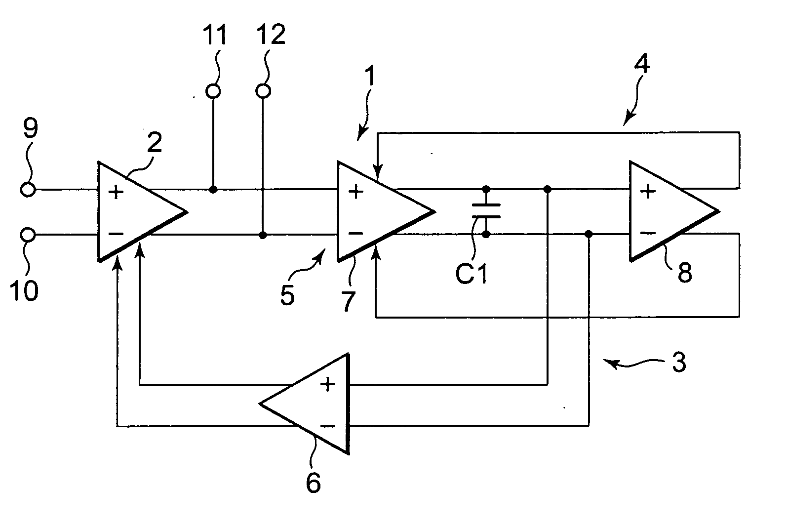
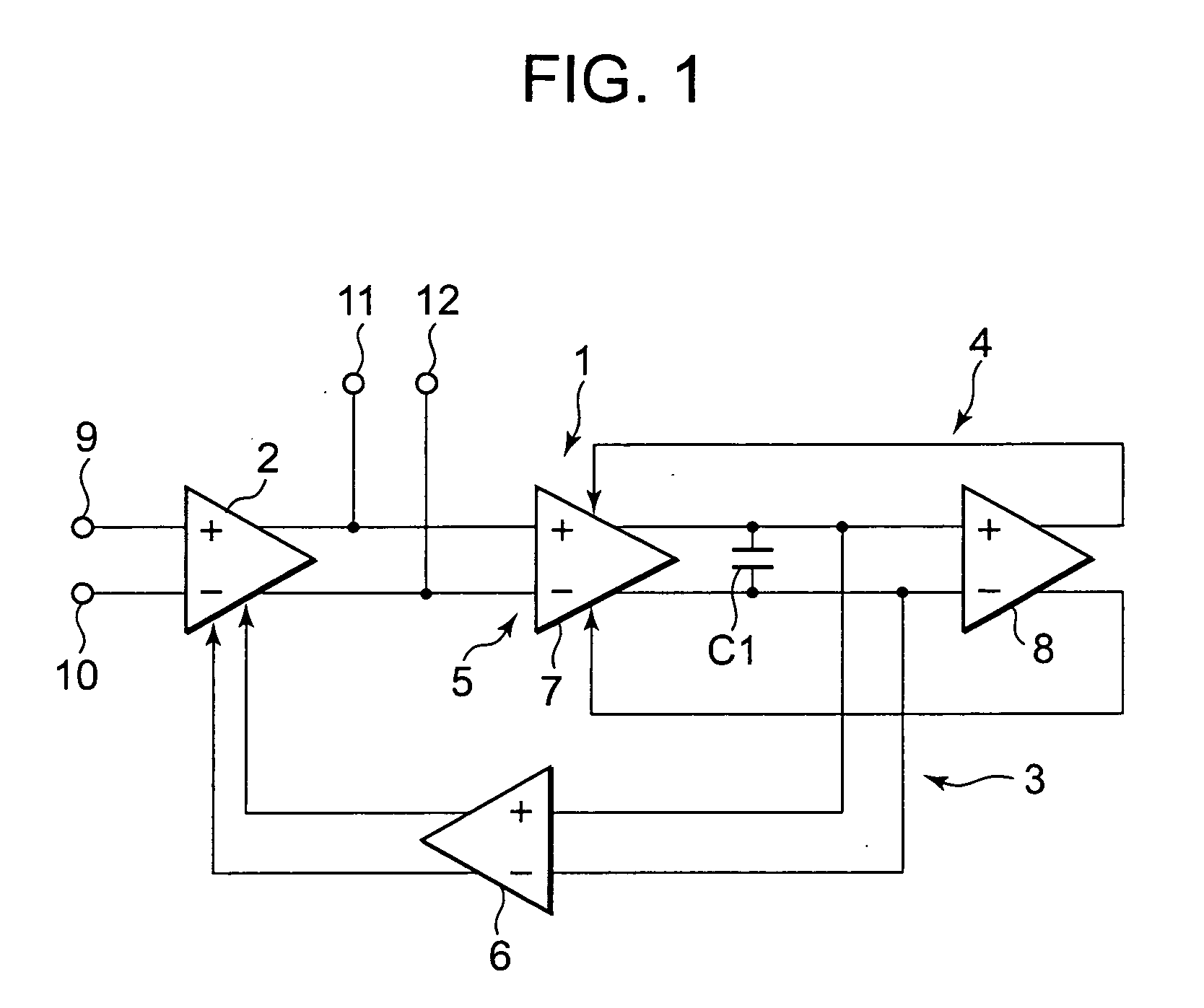
[0019] Furthermore, according to the present invention, since the gain of the positive feedback loop circuit is determined in conjunction with the gain of the negative feedback loop circuit, the gain of the positive feedback circuit can be constantly smaller than the gain of the negative feedback loop circuit, and thus, the offset voltage can be cancelled without oscillating the amplifier circuit.
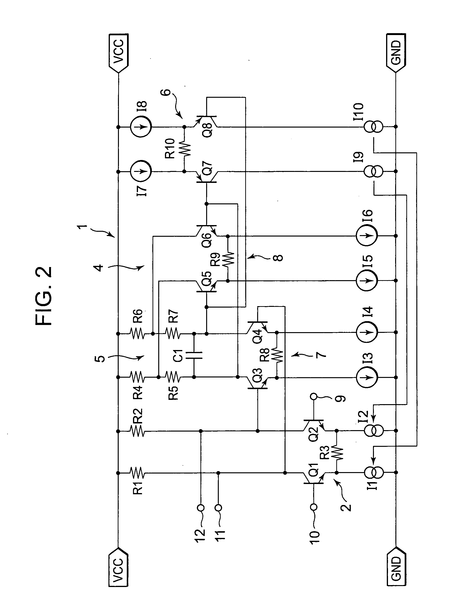
[0020] Still further, according to the present invention, since the gain of the positive feedback loop circuit is determined using some of resistors for determining the gain of the negative feedback loop circuit, an increase in circuit size of the amplifier circuit can be prevented.
[0021] Still further, according to the present invention, since, in an amplifier circuit which comprises a differential amplifier and an offset voltage canceling negative feedback loop circuit, a positive feedback loop circuit having a smaller gain than a gain of the negative feedback loop circuit is formed inside of the negative feedback loop circuit, the gain of the positive feedback loop circuit can increase a feedback amount due to the negative feedback loop circuit, so that the offset voltage of the differential amplifier can be favorably cancelled. In addition, since the gain of the positive feedback loop circuit is made smaller than the gain of the negative feedback loop circuit, the offset voltage can be cancelled without oscillating the amplifier circuit.
[0022] Still further, according to the present invention, since the gain of the positive feedback loop circuit is determined in conjunction with the gain of the negative feedback loop circuit, the gain of the positive feedback circuit can be constantly smaller than the gain of the negative feedback loop circuit, and thus the offset voltage can be cancelled without oscillating the amplifier circuit.
[0023] Still further, according to the present invention, since the gain of the positive feedback loop circuit is determined using some of resistors for determining the gain of the negative feedback loop circuit, an increase in circuit size of the amplifier circuit can be prevented.

Problems solved by technology

In the past, in a case where a differential amplifier is used as an amplifier circuit, due to slightly different properties of transistors constituting a differential pair, there has been a defect that a certain level of offset voltage is generated between output terminals of the differential amplifier, although there is no voltage difference between input terminals.

Method used


Image

  • Amplifier circuit
  • Amplifier circuit
  • Amplifier circuit

Examples


Embodiment Construction

[0028] The present invention relates to an amplifier circuit for amplifying various signals.

[0029] The amplifier circuit is constituted so as to amplify a signal by a differential amplifier, and is added with an offset cancel circuit for canceling an offset voltage of the differential amplifier. The offset cancel circuit is a negative feedback loop circuit canceling the offset voltage by amplifying and feeding back the offset voltage generated in the differential amplifier. Accordingly, the amplifier circuit of the present invention has a configuration in which the negative feedback loop circuit is connected to the differential amplifier.

[0030] In addition, in the amplifier circuit according to the present invention, there is formed a positive feedback loop circuit inside of the negative feedback loop circuit. The positive feedback loop circuit has a gain smaller than a gain of the negative feedback loop circuit.

[0031] Thus, in the present invention, since the positive feedback l...


PUM


Abstract

The present invention provides an amplifier circuit comprising a differential amplifier and a negative feedback loop circuit, in which a positive feedback loop circuit having a gain smaller than a gain of the negative feedback loop circuit is formed inside the negative feedback loop circuit.

Description

BACKGROUND OF THE INVENTION [0001] 1. Field of the Invention [0002] The present invention relates to an amplifier circuit. [0003] 2. Description of Related Art [0004] In the past, in a case where a differential amplifier is used as an amplifier circuit, due to slightly different properties of transistors constituting a differential pair, there has been a defect that a certain level of offset voltage is generated between output terminals of the differential amplifier, although there is no voltage difference between input terminals. [0005] The amplifier circuit, therefore, is designed such that a negative feedback loop circuit is connected to a differential amplifier, and that by this negative feedback loop circuit, the offset voltage of the differential amplifier is amplified and fed back to the differential amplifier, so that the offset voltage of the differential amplifier is cancelled (e.g. refer to Patent Document 1). [0006] Specifically, as illustrated in FIGS. 3 and 4, in an am...

Claims


Application Information

Patent Timeline
IPC IPC(8): H03F1/36
CPCH03F1/34H03F3/45098H03F3/45475H03F2200/129H03F2200/135H03F2203/45114H03F2203/45134H03F2203/45138H03F2203/45521H03F2203/45631H03F2203/45652H03F3/45
Inventor DAIO, KATSUHISAHIRO, TOMOYUKI
Owner SONY CORP
Learn More