
Analog/digital conversion method and analog/digital conversion circuit

Active Publication Date: 2006-05-04
SOCIONEXT INC
View PDF2 Cites 5 Cited by
  • Summary
  • Abstract
  • Description
  • Claims
  • Application Information

AI Technical Summary

Benefits of technology

[0011] The purpose of the present invention is to provide a technique for alleviating a load for processing a digital signal obtained by converting an analog signal, while maintaining the accuracy of processing the digital signal.
[0020] Changing the timing dynamically makes it possible to obtain a required digital signal at a required time. It is possible to avoid an obtainment when there is no, or low, need to obtain a digital signal. This enables a load for digital signal processing to be alleviated while maintaining an accuracy thereof gained by converting an analog signal.

Problems solved by technology

The analog signal is prone to an influence of noise, wherein influence causes AD conversion of an analog signal to be overlapped with noise.
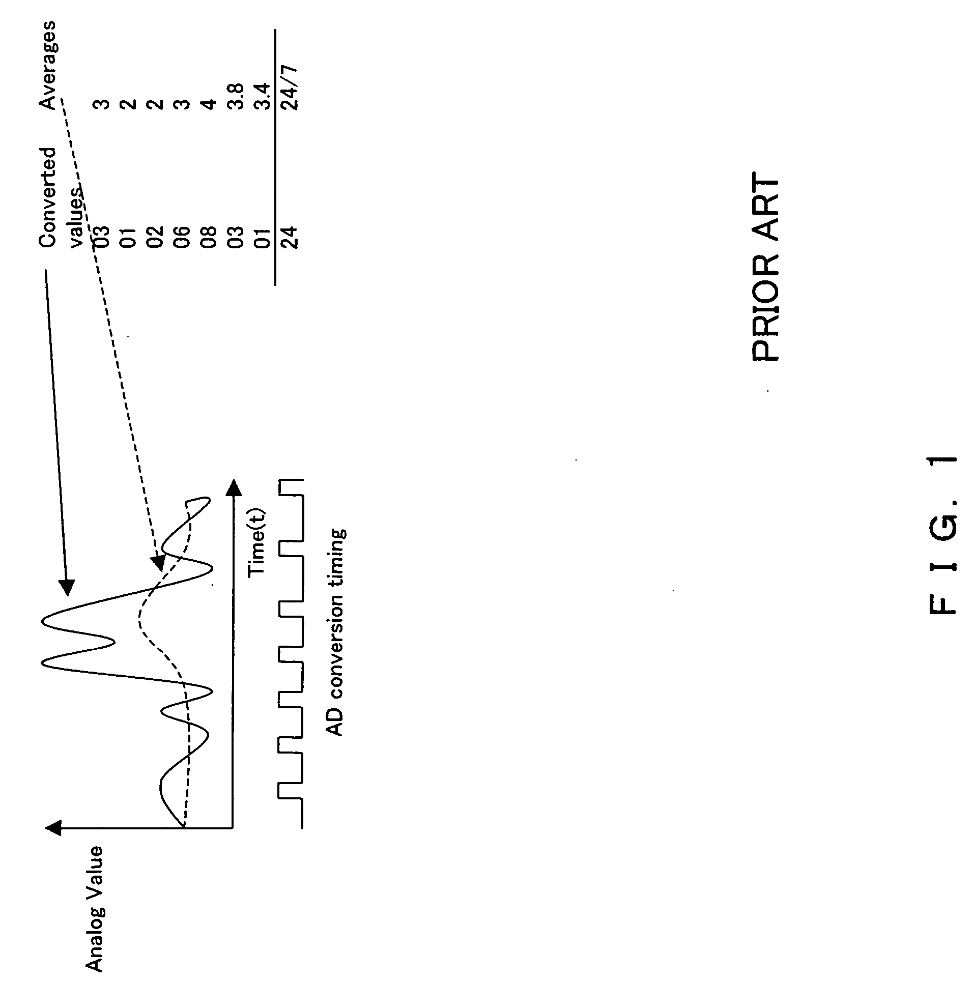
This has caused a problem of heavy load on a data processing apparatus such as CPU for processing a digital signal obtained by such a sampling.
In the conventional AD conversion circuit noted in the Japanese patent laid-open application publication No. 7-210319, however, a data processing apparatus must be disposed for the processing in dealing with a change of sampling object, because switching the switch changes the sampling object, hence further increasing the load for processing the digital signal.

Method used


Image

  • Analog/digital conversion method and analog/digital conversion circuit
  • Analog/digital conversion method and analog/digital conversion circuit
  • Analog/digital conversion method and analog/digital conversion circuit

Examples


Embodiment Construction

[0028] A preferred embodiment according to the present invention is described in the following while referring to the accompanying drawings.

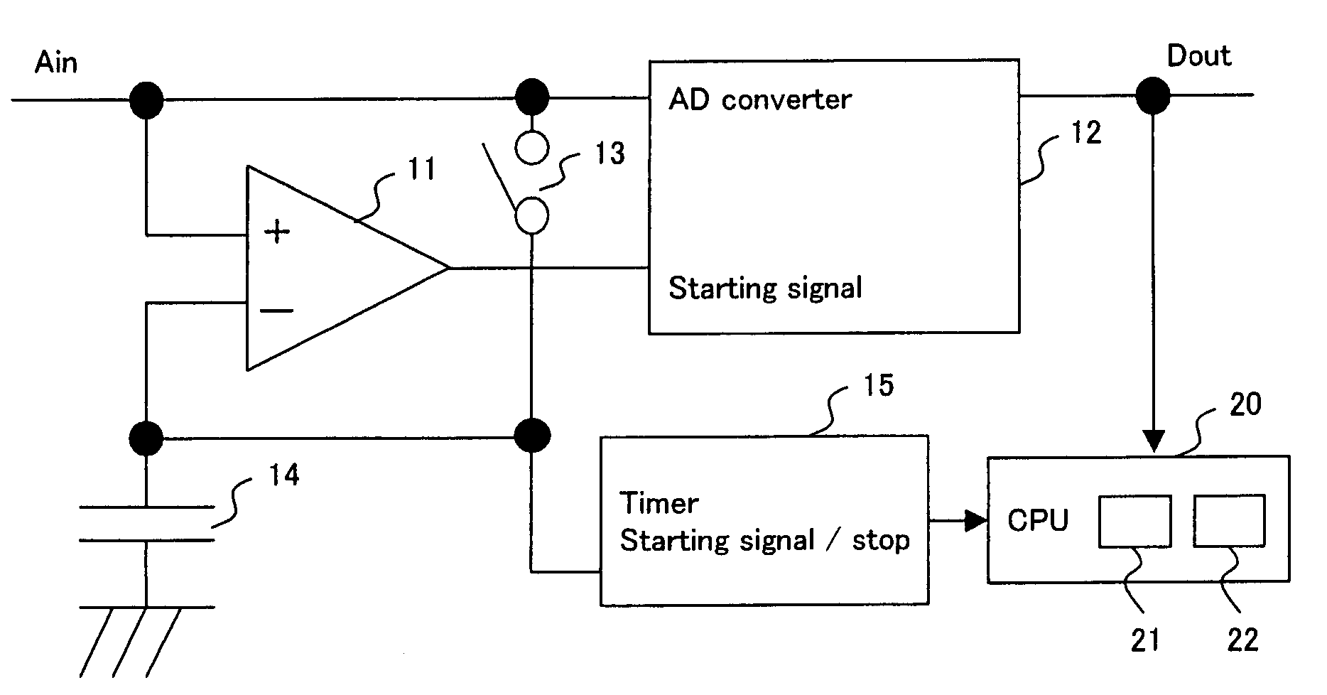
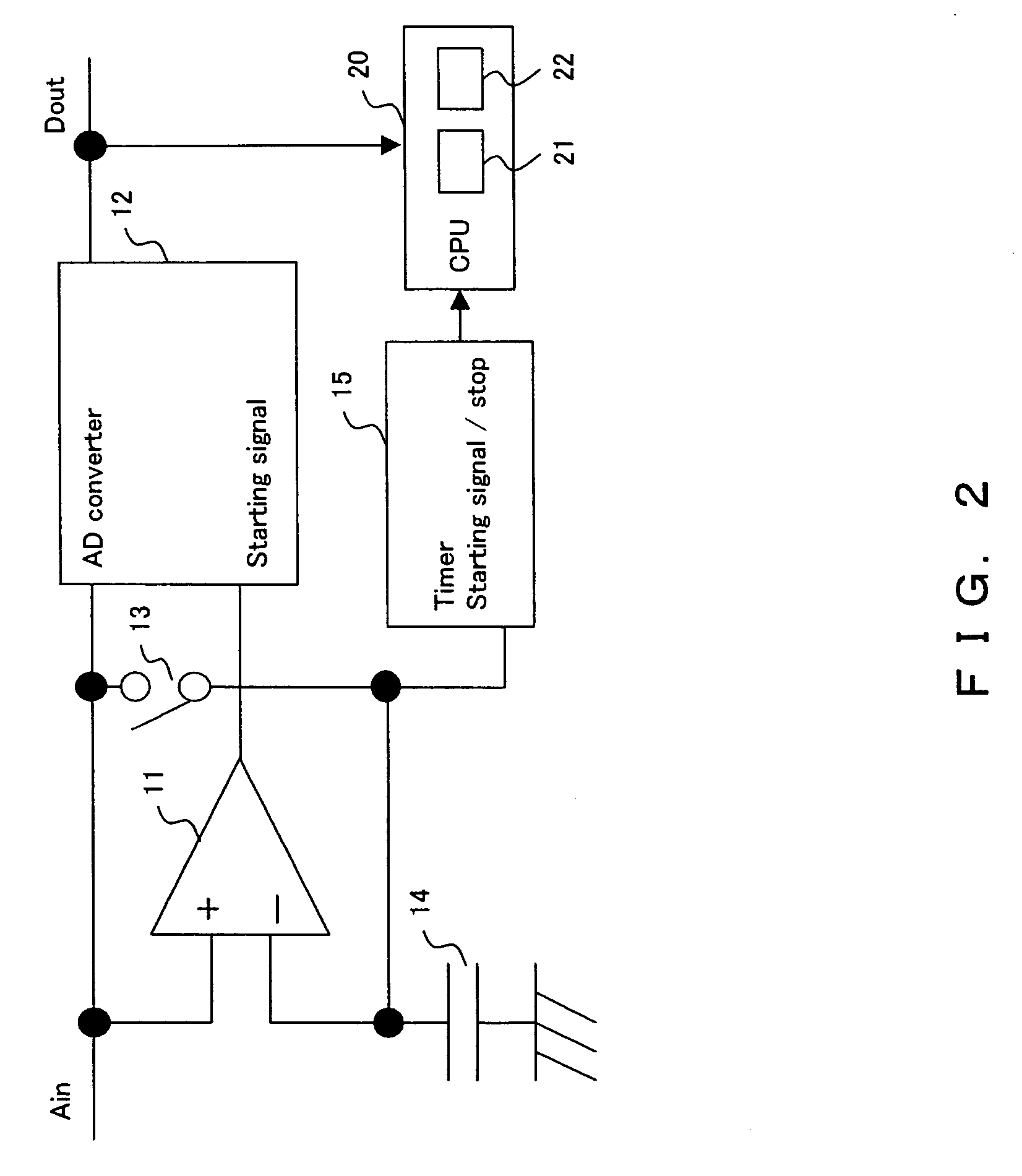
[0029]FIG. 2 describes a configuration of a sampling system applied by an AD conversion circuit according to the present embodiment. In FIG. 2, the AD conversion circuit according to the present embodiment comprises a comparator 11, an AD converter 12, a switch 13, a capacitor 14 and a timer 15.

[0030] An analog signal Ain is outputted from a not shown sensor for instance, and inputted to the AD converter 12 and the non-inversion input terminal (the plus pole) of the comparator 11. The converter 12 performs a sampling operation prompted by an output of the comparator 11 as the starting signal so as to convert the analog signal Ain to a digital signal (i.e., sampling value) Dout to output.

[0031] The switch 13 is located between the AD converter 12 and the timer 15. One of the two terminals of the capacitor 14 is connected with the ground, while...


PUM


Abstract

Paying attention to the difference between a subsequently inputted analog signal and a reference signal which is an analog signal converted to the digital signal immediately before for instance, changing timing dynamically for converting the analog signal to the digital signal, and converting an analog signal sampled at the timing of changing dynamically to a digital signal.

Description

CROSS-REFERENCE TO RELATED APPLICATIONS [0001] This application is based upon and claims the benefit of priority from the prior Japanese Patent Application No. 2004-319756, filed in Nov. 2, 2004, the entire contents of which are incorporated herein by reference. BACKGROUND OF THE INVENTION [0002] 1. Field of the Invention [0003] The present invention relates to a technique for sampling an analog signal and converting the sampled analog signal to a digital signal. [0004] 2. Description of the Related Art [0005] A lot of modern electronic equipment is configured to perform a data processing through an analog to digital conversion (“AD conversion” hereinafter) of analog signal to digital signal (i.e., digital value) to control itself. The analog signal is a sensor output for instance. [0006] The analog signal is prone to an influence of noise, wherein influence causes AD conversion of an analog signal to be overlapped with noise. This generally prompts to compute a weighted average as ...

Claims


Application Information

Patent Timeline
IPC IPC(8): H03M1/12
CPCH03M1/127
Inventor KO, SHUNICHIFUJITSUKA, AKIHIRO
Owner SOCIONEXT INC
Learn More