
Thin film transistor array substrate and method for repairing the same

a technology of thin film transistors and array substrates, applied in non-linear optics, instruments, optics, etc., can solve the problems of poor display quality of lcd and defective storage capacitors, and achieve the effect of improving manufacturing yields

Active Publication Date: 2006-05-04
AU OPTRONICS CORP
View PDF11 Cites 24 Cited by
  • Summary
  • Abstract
  • Description
  • Claims
  • Application Information

AI Technical Summary

Benefits of technology

"The present invention provides a thin film transistor array substrate and a method for repairing defective capacitors on the substrate to improve manufacturing yields and enhance the reliability of the thin film transistor array. The thin film transistor array substrate includes a plurality of scan lines, data lines, common lines, and pixel units. Each pixel unit comprises a thin film transistor, a patterned pixel electrode, and a plurality of upper electrodes. The thin film transistor is coupled to the scan line and data line corresponding to the pixel unit. The pixel electrode has at least one slit and the upper electrodes are positioned between the pixel electrode and the common line corresponding to the pixel unit. The method for repairing a defective capacitor on the substrate involves removing the portion of the pixel electrode corresponding to the defective capacitor and forming a new portion of the pixel electrode that is electrically isolated from other portions of the pixel electrode. The thin film transistor array substrate and the method for repairing defective capacitors improve manufacturing yields and reliability of the thin film transistor array."

Problems solved by technology

However, the conventional process of fabricating the thin film transistor array substrate may cause the storage capacitor defective due to process defect or other reasons. FIGS. 2A-4A are top views showing various prior art defective MIM storage capacitors. FIGS. 2B-4B are cross sectional views of the structures of FIGS. 2A-4A taken along A-A′.
Regardless which situation described above occurs, the pixel unit will not normally display and as a result the displaying quality of the LCD becomes worse.

Method used


Image

  • Thin film transistor array substrate and method for repairing the same
  • Thin film transistor array substrate and method for repairing the same
  • Thin film transistor array substrate and method for repairing the same

Examples


Embodiment Construction

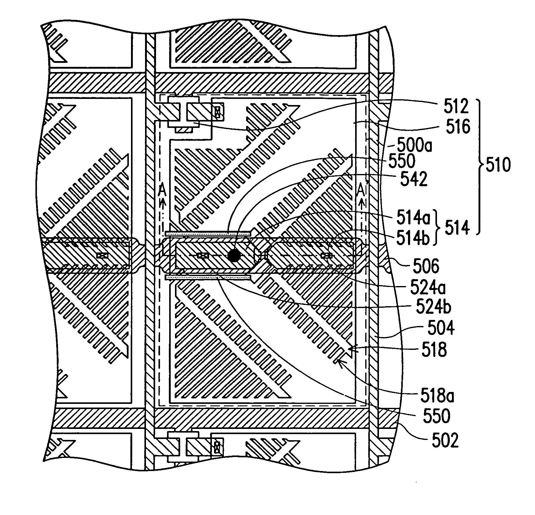
[0040]FIG. 5A is a top view of a portion of a Multi-Domain Vertical Alignment (MVA) thin film transistor array substrate according to an embodiment of the present invention. FIG. 5B is a cross sectional view of the structure of FIG. 5A taken along A-A′. Referring to FIGS. 5A and 5B, a substrate 500 can be, for example, a glass substrate. Plural scan lines 502 and plural data lines 504 are disposed over the substrate 500 to form plural pixel areas 500a on the substrate 500. In addition, plural common lines 506 are disposed over the substrate 500. The common lines 506 can be formed with the scan lines 502 in the same process, for example. The material of the common lines 506 can be, for example, chromium (Cr), aluminum (Al), or other metal with good electrical conductivity. Each common line 506 is disposed in the corresponding pixel areas 500a.

[0041] Referring to FIGS. 5A and 5B, plural pixel units 510 are disposed in one of the pixel areas 500a respectively. Each pixel unit 510 comp...


PUM

PropertyMeasurementUnit
areasaaaaaaaaaa
conductiveaaaaaaaaaa
voltagesaaaaaaaaaa

Abstract

A thin film transistor array substrate and method for repairing the same are provided. Each pixel unit of the thin film transistor array substrate has a plurality of upper electrodes, which are coupled to a common line to form a plurality of storage capacitors. If a storage capacitor defects, the portion of the pixel electrode corresponding to the defective storage capacitor is electrically isolated from the other portion of the pixel electrode in the pixel unit. Therefore, the other storage capacitors in the pixel unit can normally display. The thin film transistor array substrate and method for repairing the same provided by the present invention repair the defective storage capacitor in the thin film transistor array substrate and improve the manufacturing yield.

Description

CROSS-REFERENCE TO RELATED APPLICATION [0001] This application claims the priority benefit of Taiwan application serial no. 93133299, filed on Nov. 2, 2004. BACKGROUND OF THE INVENTION [0002] 1. Field of the Invention [0003] The present invention relates to an active device array substrate and method for repairing the same, and more particularly to a thin film transistor array substrate and method for repairing the same. [0004] 2. Description of the Related Art [0005] A thin film transistor liquid crystal display (TFT LCD) is mainly composed of a thin film transistor array substrate, a color filter array substrate and a liquid crystal layer. Wherein, the thin film transistor array substrate is composed of plural thin film transistors arranged in array and pixel electrodes corresponding to the thin film transistors. The thin film transistors serve as the switch devices of pixel units. In order to control each pixel unit, scan lines and data lines coupled to the thin film transistors ...

Claims


Application Information

Patent Timeline
Patent Type & Authority Applications(United States)
IPC IPC(8): G02F1/1343
CPCG02F1/136213G02F1/136259
Inventor HUANG, WEI-KAICHEN, YI-JENTSAI, CHEN-SHUNWANG, CHIUNG-PIN
Owner AU OPTRONICS CORP
Learn More