High-power dielectric seasoning for stable wafer-to-wafer thickness uniformity of dielectric CVD films

a dielectric cvd film, high-power technology, applied in the direction of coating, chemical vapor deposition coating, coating, etc., can solve the problems of carbon-containing gas mixture, contaminating particles that can damage or destroy semiconductor devices, and detachment from chamber components

Inactive Publication Date: 2006-05-04
APPLIED MATERIALS INC
View PDF13 Cites 486 Cited by
  • Summary
  • Abstract
  • Description
  • Claims
  • Application Information

AI Technical Summary

Benefits of technology

[0009] The present invention encompasses a method for seasoning a deposition chamber wherein one or more layers of one or more carbon-free materials are deposited on at least one internal surface of the chamber, and thereafter one or more layers of one or more organo-silicon materials are deposited on at least one substrate in the chamber. The present invention also encompasses a chamber cleaning method using low energy plasma and low pressure to remove residue from internal chamber surfaces.
[0010] In one embodiment, the seasoning method further entails depositing one or more layers of one or more carbon-containing materials over the carbon-free seasoning layer(s) before deposition of the organo-silicon layer(s). In another embodiment, the present invention encompasses a combination of the seasoning method and the cleaning method.

Problems solved by technology

This residue can also detach from the chamber components and create contaminating particles that can damage or destroy semiconductor devices.
However, such carbon-containing gas mixtures have several drawbacks.
Carbon-containing films tend to adhere strongly to these surfaces making them difficult to clean.
Residual film particles adhering to chamber walls and components, especially the faceplate, even if covered by a seasoning layer, contribute to a lack of uniformity in substrate processing.

Method used


Image

  • High-power dielectric seasoning for stable wafer-to-wafer thickness uniformity of dielectric CVD films
  • High-power dielectric seasoning for stable wafer-to-wafer thickness uniformity of dielectric CVD films
  • High-power dielectric seasoning for stable wafer-to-wafer thickness uniformity of dielectric CVD films

Examples


example 1

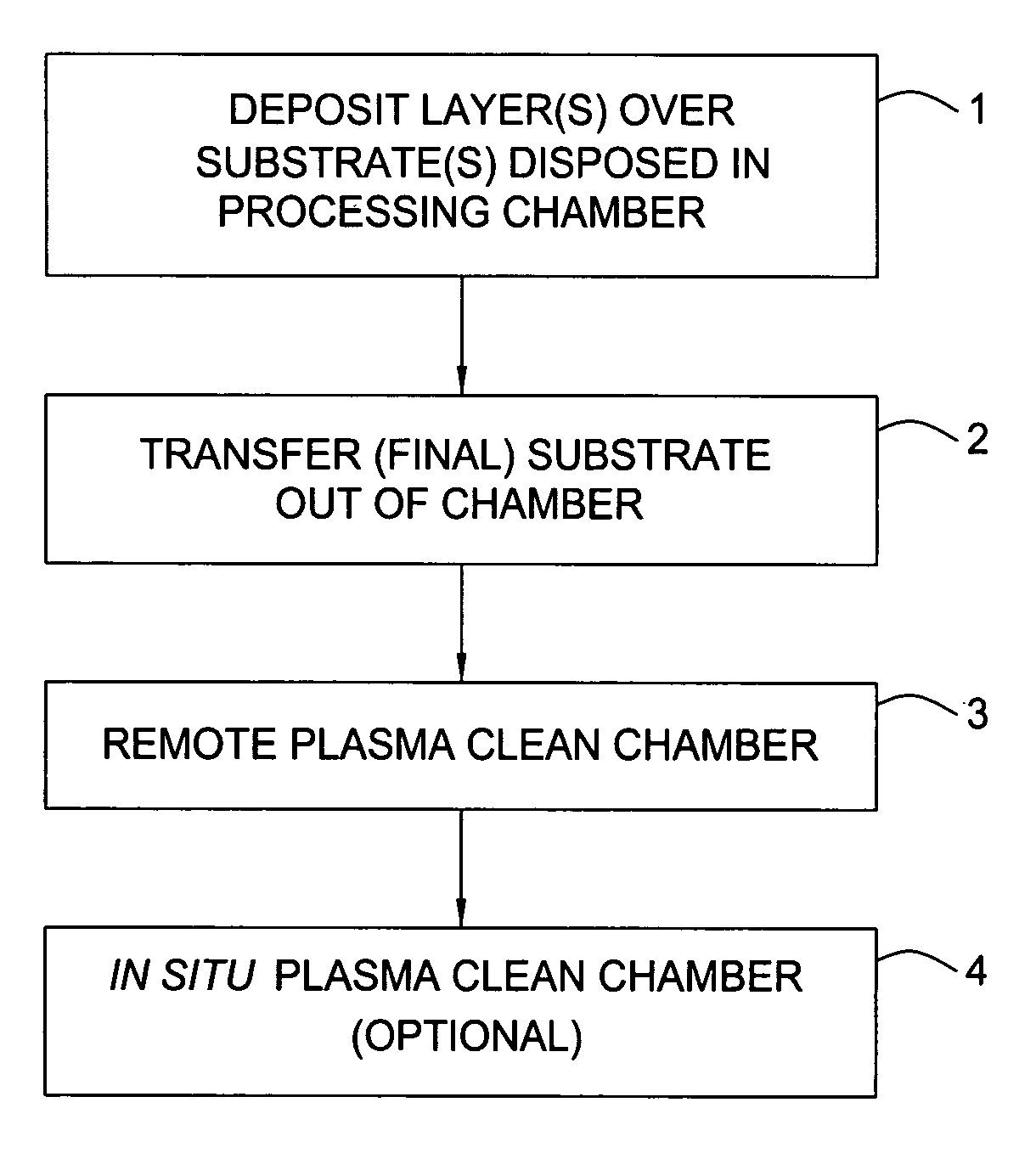
[0027] In one embodiment of the chamber cleaning method of the present invention, the cleaning process is conducted as follows: [0028] Step 1: Heat chamber to about 350° C. and commence flow of Ar [0029] Step 2: Activate remote plasma source [0030] Step 3: Commence flows of NF3, O2, and He [0031] Step 4: Cease flow of Ar and activate in situ plasma source [0032] Step 5: Cease flows of NF3, O2, and He, deactivate remote and in situ plasma sources, and evacuate chamber

The flow of Ar is begun and maintained at about 1000 sccm for about 10 seconds before the remote plasma source is activated. The RPS is maintained for about 3 seconds before the flows of NF3 (˜1000 sccm), O2 (˜500 sccm), and He (˜1000 sccm) are begun. These flows of NF3, O2, and He are maintained for about 3 seconds before the Ar flow is stopped and the in situ plasma source is activated at a power of about 150 W. These RPS / IS cleaning conditions are maintained for about 80 seconds to about 300 seconds and then the flo...

example 2

[0037] In one embodiment, a silicon nitride seasoning layer is deposited in a previously cleaned deposition chamber. A conventional CVD is carried out wherein SiH4 and N2 are provided to the chamber. The deposition chamber temperature is maintained at about 350° C. and the reactants are fed to the chamber for about 20 seconds. The RF power supplied to the chamber is about 850 to 1200 W, preferably from about 1000 to about 1200 W. Process details are as follows: [0038] Step 1: Place substrate in chamber, heat chamber to about 350° C., and commence flow of N2 [0039] Step 2: Activate in situ plasma source and commence flow of SiH4 [0040] Step 3: Cease flows of N2 and SiH4, deactivate in situ plasma source, and evacuate chamber

The flow of N2 is begun and maintained at about 18000 sccm for about 10 seconds. Then, the in situ plasma source (˜1200 W) is activated and the flow of SiH4 (˜320 sccm) is begun. These flows of N2 and SiH4 are maintained for about 20 seconds whereupon the flows ...

example 3

[0041] In another embodiment, a conventional CVD is carried out wherein SiH4, N2, and NH3 are provided to the chamber. The deposition chamber temperature is maintained at about 350° C. and the reactants are fed to the chamber for about 20 seconds. The RF power supplied to the chamber is about 850 to 1200 W, preferably from about 1000 to about 1200 W. Process details are as follows: [0042] Step 1: Place substrate in chamber, heat chamber to about 350° C., and commence flows of N2 and NH3 [0043] Step 2: Activate in situ plasma source and commence flow of SiH4 [0044] Step 3: Cease flows of N2, NH3, and SiH4, deactivate in situ plasma source, and evacuate chamber

The flow of N2 is begun and maintained at about 18000 sccm for about 10 seconds. Then, the in situ plasma source (˜1200 W) is activated and the flow of SiH4 (˜320 sccm) is begun. These flows of N2, NH3, and SiH4 are maintained for about 20 seconds whereupon the flows of N2, NH3, and SiH4 are stopped, the in situ plasma source ...


PUM

PropertyMeasurementUnit
chamber pressureaaaaaaaaaa
pressureaaaaaaaaaa
pressureaaaaaaaaaa

Abstract

A method for seasoning a deposition chamber wherein the chamber components and walls are densely coated with a material that does not contain carbon prior to deposition of an organo-silicon material on a substrate. An optional carbon-containing layer may be deposited therebetween. A chamber cleaning method using low energy plasma and low pressure to remove residue from internal chamber surfaces is provided and may be combined with the seasoning process.

Description

BACKGROUND OF THE INVENTION [0001] 1. Field of the Invention [0002] Embodiments of the present invention generally relate to the fabrication of integrated circuits. More particularly, embodiments of the invention relate to a method of seasoning the inside of a chamber and depositing a carbon-containing layer on substrates in the seasoned chamber. [0003] 2. Description of the Related Art [0004] In the fabrication of integrated circuits and semiconductor devices, low-k materials such as carbides, e.g., silicon carbide, carbon doped oxides, e.g., carbon doped silicon oxide, and carbon doped nitrides, e.g., carbon doped silicon nitride, are typically deposited on a substrate in a processing chamber, such as a deposition chamber, e.g., a chemical vapor deposition (CVD) chamber. The deposition processes typically result in deposition of some of the material on the walls and components inside the deposition chamber. The residual material deposited on the chamber walls and components can af...

Claims


Application Information

Patent Timeline
Patent Type & Authority Applications(United States)
IPC IPC(8): B05D1/36
CPCC23C16/4404C23C16/4405H01L21/3121H01L21/31633H01L21/02164H01L21/0217H01L21/02274H01L21/02301H01L21/0214H01L21/02126C23C16/40H01L21/67207C23C16/513H01L21/0262
Inventor RAJAGOPALAN, NAGARAJANXIA, LI-QUNBALSEANU, MIHAELANOWAK, THOMASSHAH, RANJANAXU, HUIWENPETERSON, CHADWITTY, DEREK R.M'SAAD, HICHEM
Owner APPLIED MATERIALS INC
Why Eureka
Try Eureka